
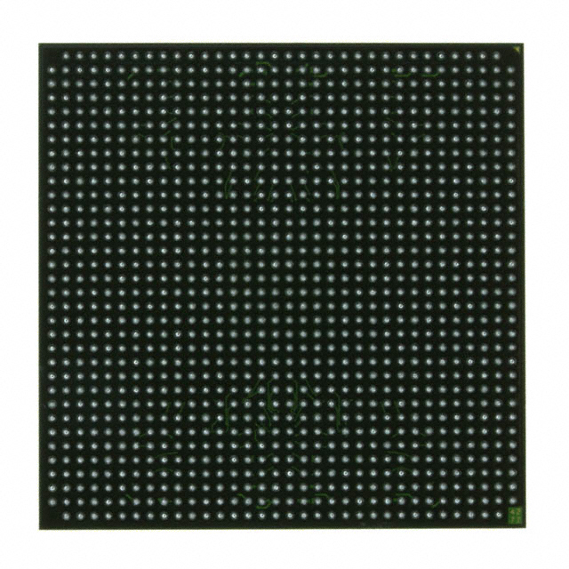
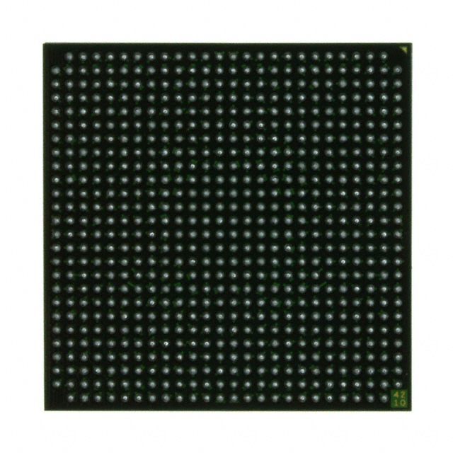
XC4VFX40-10FF672C
| Part Description |
Virtex®-4 FX Field Programmable Gate Array (FPGA) IC 352 2654208 41904 672-BBGA, FCBGA |
|---|---|
| Quantity | 335 Available (as of June 17, 2026) |

| Product Category | Field Programmable Gate Array (FPGA) |
|---|---|
| Manufacturer | AMD |
| Manufacturing Status | Active |
| Manufacturer Standard Lead Time | 12 Weeks |
| Datasheet |
Specifications & Environmental
| Device Package | 672-FCBGA (27x27) | Grade | Commercial | Operating Temperature | 0°C – 85°C | ||
|---|---|---|---|---|---|---|---|
| Package / Case | 672-BBGA, FCBGA | Number of I/O | 352 | Voltage | 1.14 V - 1.26 V | ||
| Mounting Method | Surface Mount | RoHS Compliance | RoHS non-compliant | REACH Compliance | REACH Unaffected | ||
| Moisture Sensitivity Level | 4 (72 Hours) | Number of LABs/CLBs | 4656 | Number of Logic Elements/Cells | 41904 | ||
| Number of Gates | N/A | ECCN | 3A991D | HTS Code | 8542.39.0001 | ||
| Qualification | N/A | Total RAM Bits | 2654208 |
Overview of XC4VFX40-10FF672C – Virtex®-4 FX Field Programmable Gate Array (FPGA), 672-FCBGA
The XC4VFX40-10FF672C is a Virtex®-4 FX field programmable gate array (FPGA) supplied in a 672-ball FCBGA surface-mount package. It provides a combination of logic resources, embedded memory, and I/O density suitable for commercial electronic designs requiring programmable logic integration.
Key on-chip resources include 41,904 logic elements, approximately 2.65 Mbits of embedded RAM, and 352 user I/O pins, while the device operates from a 1.14 V to 1.26 V supply and is rated for commercial temperature use (0 °C to 85 °C).
Key Features
- Logic Resources 4,656 LABs and 41,904 logic elements provide substantial on-chip programmable logic capacity for implementation of complex digital functions.
- Embedded Memory Approximately 2.65 Mbits of on-chip RAM support data buffering, state storage, and memory-intensive logic blocks without external memory.
- I/O Density 352 user I/Os enable broad interface flexibility for connecting to peripherals, sensors, and external devices.
- Power Supply Device core operates from a 1.14 V to 1.26 V supply range, matching designs that require standardized low-voltage FPGA cores.
- Package and Mounting 672-ball FCBGA (27 × 27) package in a surface-mount format supports compact board-level integration.
- Temperature Grade Commercial operating range from 0 °C to 85 °C for standard commercial applications.
- RoHS Compliance RoHS compliant for compliance with lead-free manufacturing requirements.
Typical Applications
- Prototyping and Development Use the device’s sizable logic element count and embedded RAM to implement and validate complex digital designs during system development.
- Interface and I/O Bridging High I/O pin count supports implementations that require multiple parallel and serial interfaces or protocol bridging on a single device.
- On‑chip Data Handling Approximately 2.65 Mbits of embedded memory enable local buffering and data path storage for logic functions that require on-chip RAM.
- Compact Board Integration 672-ball FCBGA surface-mount package provides a compact footprint for space-constrained PCB designs.
Unique Advantages
- Substantial Logic Capacity: 41,904 logic elements and 4,656 LABs allow integration of large logic functions without immediate partitioning across multiple devices.
- On‑Chip Memory Resources: Approximately 2.65 Mbits of embedded RAM reduce dependence on external memory for many buffering and state-storage needs.
- High I/O Count: 352 I/Os provide flexibility to support multiple interfaces and parallel connections directly from the FPGA.
- Compact FCBGA Package: 672-ball FCBGA (27 × 27) enables dense, compact designs while supporting surface-mount assembly.
- Commercial Temperature Suitability: Rated for 0 °C to 85 °C operation for standard commercial applications.
- RoHS Compliant: Facilitates use in lead-free manufacturing environments.
Why Choose XC4VFX40-10FF672C?
The XC4VFX40-10FF672C positions itself as a commercially graded Virtex-4 FX FPGA that balances logic density, embedded memory, and I/O capability in a compact FCBGA package. Its combination of 41,904 logic elements, approximately 2.65 Mbits of on-chip RAM, and 352 I/Os makes it suitable for designs that require substantial programmable logic and local memory while maintaining a small board footprint.
This device is well suited for engineers and procurement teams seeking a programmable-logic solution with clear, verifiable resources and standard commercial temperature and voltage specifications. Its RoHS compliance and surface-mount FCBGA packaging support common manufacturing flows and compact system integration.
Request a quote or submit a purchase inquiry to receive pricing and availability information for the XC4VFX40-10FF672C. Provide quantity and delivery requirements to obtain a tailored response.


Date Founded: 1969
Headquarters: Santa Clara, California, USA
Employees: 25,000+
Revenue: $22.68 Billion
Certifications and Memberships: ISO9001:2015, RoHS, REACH


