
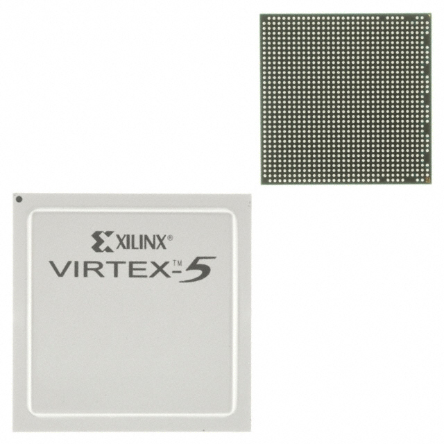
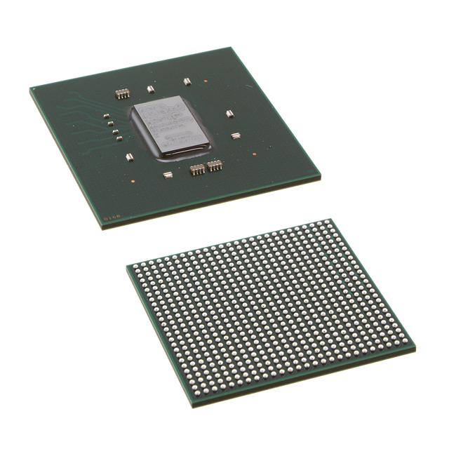
XC5VLX85-1FF676I
| Part Description |
Virtex®-5 LX Field Programmable Gate Array (FPGA) IC 440 3538944 82944 676-BBGA, FCBGA |
|---|---|
| Quantity | 716 Available (as of June 15, 2026) |

| Product Category | Field Programmable Gate Array (FPGA) |
|---|---|
| Manufacturer | AMD |
| Manufacturing Status | Active |
| Manufacturer Standard Lead Time | 12 Weeks |
| Datasheet |
Specifications & Environmental
| Device Package | 676-FCBGA (27x27) | Grade | Industrial | Operating Temperature | -40°C – 100°C | ||
|---|---|---|---|---|---|---|---|
| Package / Case | 676-BBGA, FCBGA | Number of I/O | 440 | Voltage | 950 mV - 1.05 V | ||
| Mounting Method | Surface Mount | RoHS Compliance | RoHS non-compliant | REACH Compliance | REACH Unaffected | ||
| Moisture Sensitivity Level | 4 (72 Hours) | Number of LABs/CLBs | 6480 | Number of Logic Elements/Cells | 82944 | ||
| Number of Gates | N/A | ECCN | 3A991D | HTS Code | 8542.39.0001 | ||
| Qualification | N/A | Total RAM Bits | 3538944 |
Overview of XC5VLX85-1FF676I – Virtex®-5 LX FPGA, 676‑FCBGA, Industrial Grade
The XC5VLX85-1FF676I is a Virtex®-5 LX field programmable gate array (FPGA) from AMD, supplied in a 676‑ball FCBGA package. It provides a large programmable fabric combined with significant on‑chip memory and a wide I/O complement for demanding embedded and industrial applications.
Designed for systems that require substantial logic resources, on‑chip RAM, and robust operating conditions, this device supports designs that benefit from a high logic element count, extensive I/O, and an industrial temperature range.
Key Features
- Programmable Logic Capacity Approximately 82,944 logic elements suitable for complex custom logic implementations and parallel processing architectures.
- Embedded Memory Approximately 3.538944 Mbits of on‑chip RAM, enabling local buffering, FIFOs, and data‑path storage without external memory in many designs.
- I/O Resources 440 user I/O pins to support wide buses, multiple interfaces, and flexible connectivity options for peripherals and daughtercards.
- Power Supply Core supply range of 0.95 V to 1.05 V to match system power‑rail requirements and enable predictable power sequencing.
- Package and Mounting 676‑ball FCBGA (27 × 27 mm) surface‑mount package for high‑density board integration and reliable soldered connections.
- Industrial Temperature Range Rated for operation from −40 °C to 100 °C, supporting extended temperature environments common in industrial and ruggedized systems.
- Compliance RoHS compliant, meeting common environmental requirements for lead‑free assembly.
Typical Applications
- Industrial Control Implement real‑time control logic, motor control interfaces, and deterministic I/O handling that leverage the device’s industrial temperature rating and large I/O count.
- Signal Processing Use the extensive logic fabric and embedded RAM for data path acceleration, filtering, and custom DSP pipelines.
- Prototyping and Custom Hardware Deploy as a platform for hardware prototyping, algorithm validation, and custom accelerators where high logic density and flexible I/O are required.
- Embedded System Integration Integrate multiple peripheral interfaces and custom state machines directly in the FPGA fabric to reduce external component count.
Unique Advantages
- Large Logic Capacity: With approximately 82,944 logic elements, the device supports complex designs and substantial parallelism without immediate need for multiple FPGAs.
- On‑Chip Memory: Nearly 3.54 Mbits of embedded RAM reduce dependence on external memory for buffering and local storage, simplifying board design.
- Extensive I/O Count: 440 I/O pins enable direct connection to a wide range of peripherals, high‑speed interfaces, and wide data buses.
- Industrial Reliability: Rated for −40 °C to 100 °C operation, the part is suitable for deployments in harsh or wide‑temperature industrial environments.
- High‑Density Packaging: The 676‑FCBGA (27 × 27 mm) package delivers a compact, soldered solution for high‑pin‑count requirements while supporting surface‑mount assembly.
- Standards‑Friendly Compliance: RoHS compliance supports lead‑free manufacturing and regulatory requirements for many markets.
Why Choose XC5VLX85-1FF676I?
The XC5VLX85-1FF676I combines a large programmable fabric, substantial embedded memory, and a broad I/O complement in a single industrial‑rated FCBGA package. This combination makes it well suited to designers who need significant on‑chip resources and reliable operation across a wide temperature range.
Ideal for development teams and production designs that require scalable logic capacity, on‑chip buffering, and robust board‑level integration, the device provides a clear platform for consolidating functions and simplifying system architecture while meeting environmental and assembly requirements.
Request a quote or contact our sales team to discuss availability, volume pricing, and technical support for the XC5VLX85-1FF676I.


Date Founded: 1969
Headquarters: Santa Clara, California, USA
Employees: 25,000+
Revenue: $22.68 Billion
Certifications and Memberships: ISO9001:2015, RoHS, REACH


