
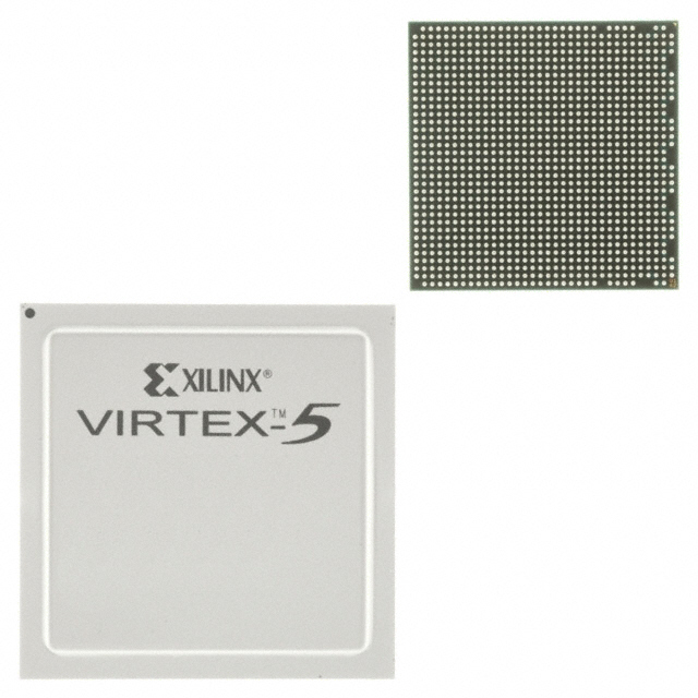
XC5VLX85-1FFG676C
| Part Description |
Virtex®-5 LX Field Programmable Gate Array (FPGA) IC 440 3538944 82944 676-BBGA, FCBGA |
|---|---|
| Quantity | 424 Available (as of June 15, 2026) |

| Product Category | Field Programmable Gate Array (FPGA) |
|---|---|
| Manufacturer | AMD |
| Manufacturing Status | Active |
| Manufacturer Standard Lead Time | 12 Weeks |
| Datasheet |
Specifications & Environmental
| Device Package | 676-FCBGA (27x27) | Grade | Commercial | Operating Temperature | 0°C – 85°C | ||
|---|---|---|---|---|---|---|---|
| Package / Case | 676-BBGA, FCBGA | Number of I/O | 440 | Voltage | 950 mV - 1.05 V | ||
| Mounting Method | Surface Mount | RoHS Compliance | ROHS3 Compliant | REACH Compliance | REACH Unaffected | ||
| Moisture Sensitivity Level | 4 (72 Hours) | Number of LABs/CLBs | 6480 | Number of Logic Elements/Cells | 82944 | ||
| Number of Gates | N/A | ECCN | 3A991D | HTS Code | 8542.39.0001 | ||
| Qualification | N/A | Total RAM Bits | 3538944 |
Overview of XC5VLX85-1FFG676C – Virtex®-5 LX FPGA, 676‑FCBGA, 440 I/O
The XC5VLX85-1FFG676C is a Virtex®-5 LX Field Programmable Gate Array (FPGA) from AMD. It integrates 82,944 logic elements with approximately 3.54 Mbits of on-chip RAM and provides 440 user I/O in a compact 676‑FCBGA (27×27) package.
Designed for complex digital logic implementations and high-density I/O designs, this commercial-grade, surface-mount FPGA supports a 0.95–1.05 V core voltage range and an operating temperature range of 0 °C to 85 °C, offering a balance of capacity, integration, and manufacturability for demanding embedded applications.
Key Features
- Core Capacity 82,944 logic elements for implementing large-scale digital designs and parallel logic functions.
- Embedded Memory Approximately 3.54 Mbits of on-chip RAM to support buffering, lookup tables, and data storage inside the FPGA fabric.
- High‑Density I/O 440 user I/O pins to accommodate wide bus interfaces, multiple signaling channels, and flexible peripheral connections.
- Power Core supply range of 0.95 V to 1.05 V to match system power-rail requirements and support standard FPGA power domains.
- Package & Mounting 676‑FCBGA (27×27) package in a surface-mount form factor for compact board-level integration.
- Operating Conditions Commercial grade device with an operating temperature range of 0 °C to 85 °C suitable for temperature-controlled environments.
- Compliance RoHS‑compliant to meet standard environmental regulations for lead-free manufacturing.
Typical Applications
- High‑density I/O systems Use the 440 user I/O to interface with multiple parallel buses, front-end controllers, or high-channel-count peripherals.
- Memory‑intensive logic Leverage approximately 3.54 Mbits of embedded memory for buffering, packet processing, and temporary data storage inside the FPGA.
- Complex digital designs Deploy the 82,944 logic elements for large combinational and sequential logic blocks, state machines, and custom accelerators.
Unique Advantages
- Substantial logic resources: 82,944 logic elements enable implementation of large and complex digital functions without immediate need for multiple devices.
- On‑chip memory availability: Approximately 3.54 Mbits of embedded RAM reduces external memory dependence and simplifies board-level design.
- Extensive I/O count: 440 user I/O pins support broad interfacing options and reduce the need for additional I/O expanders.
- Compact, manufacturable package: 676‑FCBGA (27×27) surface-mount package supports dense PCB layouts and automated assembly processes.
- Commercial temperature range: 0 °C to 85 °C aligns with general-purpose electronics and system-level thermal designs.
- RoHS compliant: Meets lead-free manufacturing requirements for modern production environments.
Why Choose XC5VLX85-1FFG676C?
The XC5VLX85-1FFG676C positions itself as a high-capacity Virtex‑5 LX FPGA offering a strong balance of logic density, embedded memory, and I/O resources in a single commercial-grade package. Its combination of 82,944 logic elements, approximately 3.54 Mbits of on-chip RAM, and 440 I/O pins makes it suitable for designs that require substantial internal resources and broad interfacing capability.
This device is well suited to engineering teams building medium- to large-scale digital systems that require on-chip memory and high I/O counts while maintaining standard commercial operating conditions and surface-mount board assembly practices. Manufacturer documentation is available for detailed implementation and system integration guidance.
Request a quote or submit an inquiry to get pricing and availability details for the XC5VLX85-1FFG676C.


Date Founded: 1969
Headquarters: Santa Clara, California, USA
Employees: 25,000+
Revenue: $22.68 Billion
Certifications and Memberships: ISO9001:2015, RoHS, REACH


