
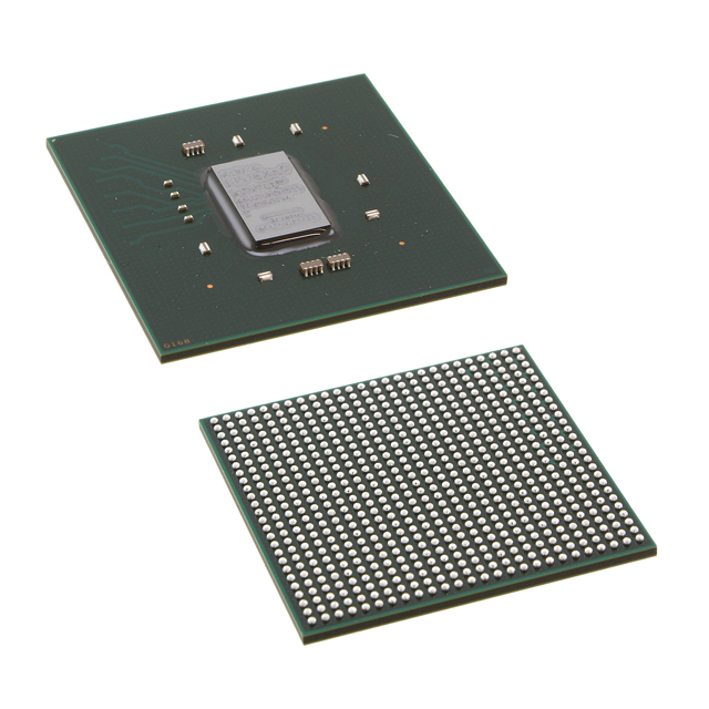
XC5VLX85-2FFG676C
| Part Description |
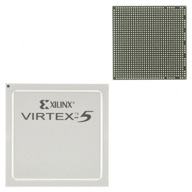
Virtex®-5 LX Field Programmable Gate Array (FPGA) IC 440 3538944 82944 676-BBGA, FCBGA |
|---|---|
| Quantity | 1,007 Available (as of June 18, 2026) |

| Product Category | Field Programmable Gate Array (FPGA) |
|---|---|
| Manufacturer | AMD |
| Manufacturing Status | Active |
| Manufacturer Standard Lead Time | 12 Weeks |
| Datasheet |
Specifications & Environmental
| Device Package | 676-FCBGA (27x27) | Grade | Commercial | Operating Temperature | 0°C – 85°C | ||
|---|---|---|---|---|---|---|---|
| Package / Case | 676-BBGA, FCBGA | Number of I/O | 440 | Voltage | 950 mV - 1.05 V | ||
| Mounting Method | Surface Mount | RoHS Compliance | ROHS3 Compliant | REACH Compliance | REACH Unaffected | ||
| Moisture Sensitivity Level | 4 (72 Hours) | Number of LABs/CLBs | 6480 | Number of Logic Elements/Cells | 82944 | ||
| Number of Gates | N/A | ECCN | 3A991D | HTS Code | 8542.39.0001 | ||
| Qualification | N/A | Total RAM Bits | 3538944 |
Overview of XC5VLX85-2FFG676C – Virtex®-5 LX Field Programmable Gate Array, 676-FCBGA
The XC5VLX85-2FFG676C is a Virtex®-5 LX Field Programmable Gate Array (FPGA) from AMD. It provides a high-capacity logic fabric with dedicated on-chip memory and a large I/O count in a 676-ball FCBGA package for surface-mount applications.
Targeted for commercial-grade designs, this device combines 6,480 CLBs and 82,944 logic elements with approximately 3.54 Mbits of embedded memory, supporting complex digital systems that require dense logic integration and flexible I/O.
Key Features
- Logic Capacity 6,480 CLBs totaling 82,944 logic elements for implementing large-scale digital logic and custom processing blocks.
- Embedded Memory Approximately 3.54 Mbits of on-chip RAM to support FIFOs, buffers, and memory-intensive logic functions.
- I/O Resources 440 user I/O pins to interface with a wide range of external devices, sensors, and peripherals.
- Power Supply Core voltage range of 950 mV to 1.05 V to match system power rails and regulator designs.
- Package and Mounting 676-FCBGA (27×27) ball grid array in a surface-mount package for high-density board layouts.
- Operating Range Commercial temperature grade rated from 0 °C to 85 °C for standard commercial environments.
- Compliance RoHS compliant for adherence to common environmental requirements.
Typical Applications
- High-density digital processing Large logic capacity and abundant I/Os support complex custom processors, state machines, and logic consolidation in multi-function systems.
- Memory-centric designs Approximately 3.54 Mbits of embedded RAM enables on-chip buffering, packet queuing, and other memory-dependent functions without immediate external RAM.
- Interface consolidation With 440 I/Os, the device can bridge multiple external interfaces, peripherals, and sensors on a single FPGA fabric.
Unique Advantages
- Substantial logic resources: 6,480 CLBs and 82,944 logic elements allow designers to implement large and complex logic functions on a single device, reducing the need for multiple FPGAs.
- On-chip memory: Approximately 3.54 Mbits of embedded RAM supports data buffering and local storage, simplifying board-level memory requirements.
- Extensive I/O availability: 440 user I/Os provide flexibility for system integration and reduce the need for external multiplexing or I/O expanders.
- Compact package: 676-FCBGA (27×27) surface-mount package supports high-density PCB designs while delivering the device’s full I/O and logic capacity.
- Commercial temperature grade: Rated for 0 °C to 85 °C operation, suitable for standard commercial electronics applications.
- RoHS compliant: Meets environmental compliance requirements for many global markets.
Why Choose XC5VLX85-2FFG676C?
The XC5VLX85-2FFG676C positions itself as a high-capacity Virtex®-5 LX FPGA suitable for commercial designs that demand extensive logic, significant on-chip memory, and a large complement of I/Os in a compact FCBGA package. Its combination of CLB count, embedded RAM, and 440 I/Os makes it appropriate for consolidating complex digital functions and interface logic onto a single device.
Designed by AMD, this FPGA offers a balance of integration and flexibility for engineering teams developing scalable digital systems where board space and I/O density are key considerations. Detailed device documentation is available to support evaluation and integration into your designs.
Request a quote or submit an inquiry to get pricing and availability for the XC5VLX85-2FFG676C.


Date Founded: 1969
Headquarters: Santa Clara, California, USA
Employees: 25,000+
Revenue: $22.68 Billion
Certifications and Memberships: ISO9001:2015, RoHS, REACH


