
XC7A15T-L2CSG324E
| Part Description |
Artix-7 Field Programmable Gate Array (FPGA) IC 210 921600 16640 324-LFBGA, CSPBGA |
|---|---|
| Quantity | 233 Available (as of June 15, 2026) |

| Product Category | Field Programmable Gate Array (FPGA) |
|---|---|
| Manufacturer | AMD |
| Manufacturing Status | Active |
| Manufacturer Standard Lead Time | 16 Weeks |
| Datasheet |
Specifications & Environmental
| Device Package | 324-CSPBGA (15x15) | Grade | Extended | Operating Temperature | 0°C – 100°C | ||
|---|---|---|---|---|---|---|---|
| Package / Case | 324-LFBGA, CSPBGA | Number of I/O | 210 | Voltage | 950 mV - 1.05 V | ||
| Mounting Method | Surface Mount | RoHS Compliance | ROHS3 Compliant | REACH Compliance | REACH Unaffected | ||
| Moisture Sensitivity Level | 3 (168 Hours) | Number of LABs/CLBs | 1300 | Number of Logic Elements/Cells | 16640 | ||
| Number of Gates | N/A | ECCN | 3A991D | HTS Code | 8542.39.0001 | ||
| Qualification | N/A | Total RAM Bits | 921600 |
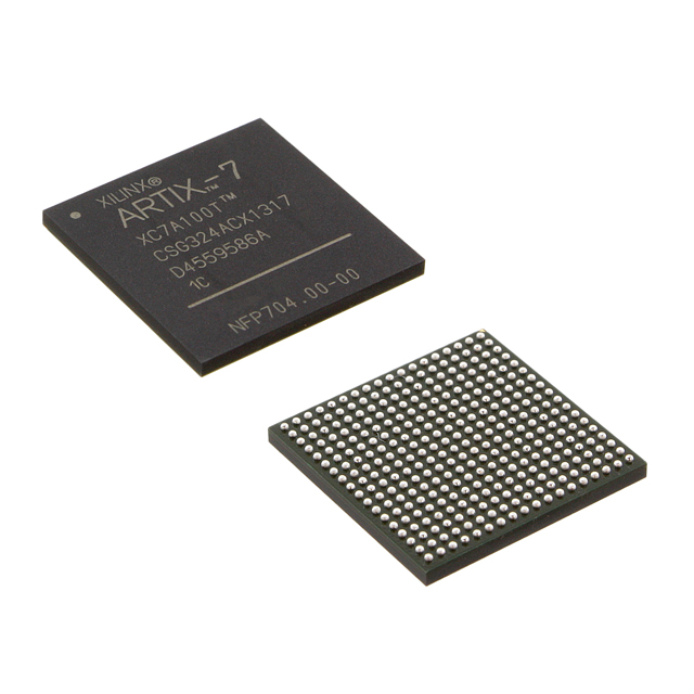
Overview of XC7A15T-L2CSG324E – Artix‑7 FPGA, 16,640 logic elements, 210 I/O, 324‑LFBGA
The XC7A15T-L2CSG324E is an Artix‑7 field programmable gate array (FPGA) IC from AMD. It provides mid‑range programmable logic capacity with on‑chip embedded memory and a substantial I/O count in a compact 324‑LFBGA (324‑CSPBGA, 15×15) surface‑mount package. This device is targeted at designs that require configurable digital logic, embedded RAM, and a high number of I/O signals within a single chip.
Key Features
- Logic Capacity – 1,300 CLBs with 16,640 logic elements (cells) to implement custom digital functions and finite state machines.
- Embedded Memory – Approximately 0.92 Mbits of on‑chip RAM (921,600 total RAM bits) for buffers, FIFOs, and small data storage.
- I/O Density – 210 user I/O pins to support a wide range of external interfaces and parallel connections.
- Package & Mounting – 324‑LFBGA (supplier package: 324‑CSPBGA, 15×15) in a surface‑mount form factor for compact board integration.
- Power – Core voltage supply range specified from 950 mV to 1.05 V to match system power rails.
- Temperature & Grade – Extended grade device with an operating temperature range of 0°C to 100°C.
- Compliance – RoHS compliant, supporting regulatory requirements for lead‑free assembly.
Typical Applications
- Programmable Logic and Prototyping – Implement custom digital logic, algorithm testing, and hardware prototyping where reconfigurable logic is needed.
- I/O Expansion and Interface Bridging – Use the 210 I/O pins to bridge or aggregate multiple peripheral interfaces and perform protocol translation.
- Embedded Memory‑Assisted Designs – Leverage approximately 0.92 Mbits of on‑chip RAM for buffering, small lookup tables, and temporary data storage within signal processing or control paths.
Unique Advantages
- Balanced Logic and Memory: 16,640 logic elements paired with approximately 0.92 Mbits of embedded RAM enables versatile mid‑range designs without external memory for many use cases.
- High I/O Count: 210 I/O pins provide flexibility for connecting sensors, peripherals, buses, and custom interface circuitry.
- Compact Surface‑Mount Package: 324‑LFBGA (324‑CSPBGA, 15×15) minimizes PCB footprint while providing necessary pin density for complex designs.
- Controlled Power Envelope: Core voltage specified between 950 mV and 1.05 V to align with modern low‑voltage system designs.
- Extended Grade Operation: Rated for 0°C to 100°C operation to suit applications requiring extended temperature range performance.
- Regulatory Compliance: RoHS compliance supports lead‑free manufacturing and global environmental requirements.
Why Choose XC7A15T-L2CSG324E?
The XC7A15T-L2CSG324E positions itself as a mid‑range Artix‑7 FPGA option that combines a meaningful logic element count, embedded RAM capacity, and a high I/O complement in a compact 324‑LFBGA package. Its extended grade temperature range and RoHS compliance make it suitable for a variety of commercial and industrial applications that require reliable, reconfigurable logic and on‑chip memory.
This device is appropriate for designers seeking a single‑chip programmable solution to implement custom logic, interface aggregation, and memory‑assisted processing while maintaining a small PCB footprint and defined power requirements.
Request a quote or submit an inquiry to receive pricing and availability information for the XC7A15T-L2CSG324E. Provide your project details and quantity requirements to expedite the response.


Date Founded: 1969
Headquarters: Santa Clara, California, USA
Employees: 25,000+
Revenue: $22.68 Billion
Certifications and Memberships: ISO9001:2015, RoHS, REACH


