
XCKU9P-L1FFVE900I
| Part Description |
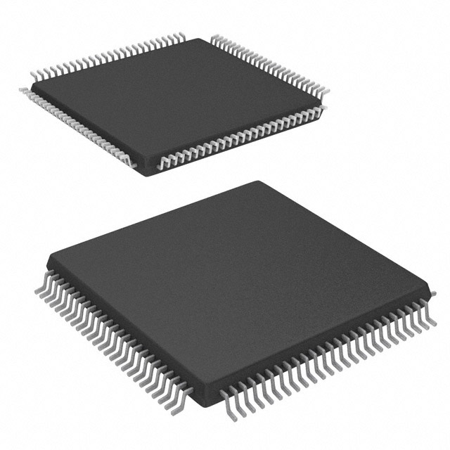
Kintex® UltraScale+™ Field Programmable Gate Array (FPGA) IC 304 41881600 599550 900-BBGA, FCBGA |
|---|---|
| Quantity | 1,084 Available (as of June 18, 2026) |

| Product Category | Field Programmable Gate Array (FPGA) |
|---|---|
| Manufacturer | AMD |
| Manufacturing Status | Active |
| Manufacturer Standard Lead Time | 16 Weeks |
| Datasheet |
Specifications & Environmental
| Device Package | 900-FCBGA (31x31) | Grade | Industrial | Operating Temperature | -40°C – 100°C | ||
|---|---|---|---|---|---|---|---|
| Package / Case | 900-BBGA, FCBGA | Number of I/O | 304 | Voltage | 698 mV - 876 mV | ||
| Mounting Method | Surface Mount | RoHS Compliance | ROHS3 Compliant | REACH Compliance | REACH Unknown | ||
| Moisture Sensitivity Level | 4 (72 Hours) | Number of LABs/CLBs | 34260 | Number of Logic Elements/Cells | 599550 | ||
| Number of Gates | N/A | ECCN | 3A991D | HTS Code | 8542.39.0001 | ||
| Qualification | N/A | Total RAM Bits | 41881600 |
Overview of XCKU9P-L1FFVE900I – Kintex® UltraScale+™ FPGA, 599,550 Logic Elements, 900‑FCBGA
The XCKU9P-L1FFVE900I is a Kintex® UltraScale+™ field programmable gate array (FPGA) from AMD, offered in a 900‑ball FCBGA package. It provides a high logic capacity and substantial on‑chip memory in a compact surface‑mount package for industrial applications.
With 599,550 logic elements, approximately 42 Mbits of embedded memory and 304 I/O, this device is suited for designs that require dense logic resources, significant embedded RAM and numerous interface pins while operating over an industrial temperature range.
Key Features
- Core Logic 599,550 logic elements and 34,260 CLBs provide a high logic resource count for complex digital designs.
- Embedded Memory Approximately 42 Mbits of on‑chip RAM (41,881,600 bits) to support large buffers, FIFOs and local data storage.
- I/O Resources 304 I/O pins to support multiple interfaces and high pin‑count connectivity options.
- Power Supply Core voltage supply range from 698 mV to 876 mV enabling integration with modern low‑voltage power rails.
- Package & Mounting 900‑FCBGA (31 × 31 mm) package, surface mount, offering a high‑pin‑count, compact footprint.
- Operating Range & Grade Industrial grade device with an operating temperature range of −40 °C to 100 °C for demanding environments.
- Environmental Compliance RoHS compliant to meet standard environmental regulations for electronic components.
Typical Applications
- High‑density digital signal processing Use the large logic array and abundant embedded memory for DSP pipelines, filtering and real‑time processing tasks.
- Data and packet processing Leverage the combination of logic resources and on‑chip RAM to implement packet buffering, parsing and custom acceleration functions.
- Communications infrastructure Utilize the 304 I/O pins and high logic capacity to implement protocol processing, interface bridging and multiport I/O designs.
- Industrial control and automation Deploy in systems that require industrial temperature operation and robust, high‑capacity programmable logic for control algorithms and I/O aggregation.
Unique Advantages
- High logic capacity: 599,550 logic elements enable implementation of complex SoC‑class functions and large FPGA designs without partitioning across multiple devices.
- Significant embedded memory: Approximately 42 Mbits of on‑chip RAM reduce external memory dependencies and simplify high‑bandwidth buffering needs.
- Generous I/O count: 304 I/O pins provide flexibility for multi‑lane interfaces, peripheral connectivity and mixed signal routing.
- Industrial temperature rating: Rated for −40 °C to 100 °C to support deployment in harsh or temperature‑variable environments.
- Compact, high‑pin‑count package: 900‑FCBGA (31 × 31 mm) offers a small footprint while maintaining a high number of connections for dense system integration.
- Low‑voltage core support: Core voltage range of 698 mV to 876 mV aligns with modern low‑power supply architectures.
Why Choose XCKU9P-L1FFVE900I?
The XCKU9P-L1FFVE900I combines a large logic fabric, substantial embedded memory and a high I/O count in a 900‑ball FCBGA package, providing a balanced platform for complex, memory‑intensive and I/O‑rich designs. As an industrial‑grade Kintex® UltraScale+™ FPGA from AMD, it is positioned for designs that require scalable logic resources with consistent operating range and environmental compliance.
This device is suited for engineering teams building high‑performance processing, communications or industrial control systems that need on‑chip memory, dense logic and numerous interfaces in a compact surface‑mount form factor.
Request a quote or submit a request for pricing and availability to evaluate the XCKU9P-L1FFVE900I for your next design project.


Date Founded: 1969
Headquarters: Santa Clara, California, USA
Employees: 25,000+
Revenue: $22.68 Billion
Certifications and Memberships: ISO9001:2015, RoHS, REACH


