
XCKU9P-2FFVE900I
| Part Description |
Kintex® UltraScale+™ Field Programmable Gate Array (FPGA) IC 304 41881600 599550 900-BBGA, FCBGA |
|---|---|
| Quantity | 219 Available (as of October 7, 2026) |

| Product Category | Field Programmable Gate Array (FPGA) |
|---|---|
| Manufacturer | AMD |
| Manufacturing Status | Active |
| Manufacturer Standard Lead Time | 16 Weeks |
| Datasheet |
Specifications & Environmental
| Device Package | 900-FCBGA (31x31) | Grade | Industrial | Operating Temperature | -40°C – 100°C | ||
|---|---|---|---|---|---|---|---|
| Package / Case | 900-BBGA, FCBGA | Number of I/O | 304 | Voltage | 825 mV - 876 mV | ||
| Mounting Method | Surface Mount | RoHS Compliance | ROHS3 Compliant | REACH Compliance | REACH Unknown | ||
| Moisture Sensitivity Level | 4 (72 Hours) | Number of LABs/CLBs | 34260 | Number of Logic Elements/Cells | 599550 | ||
| Number of Gates | N/A | ECCN | 3A991D | HTS Code | 8542.39.0001 | ||
| Qualification | N/A | Total RAM Bits | 41881600 |
Overview of XCKU9P-2FFVE900I – Kintex® UltraScale+™ Field Programmable Gate Array (FPGA), 900‑FCBGA, Industrial Grade
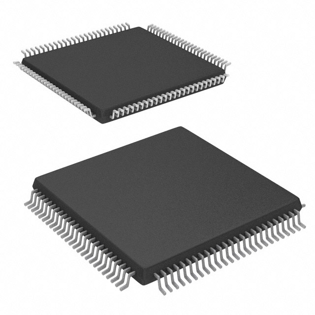
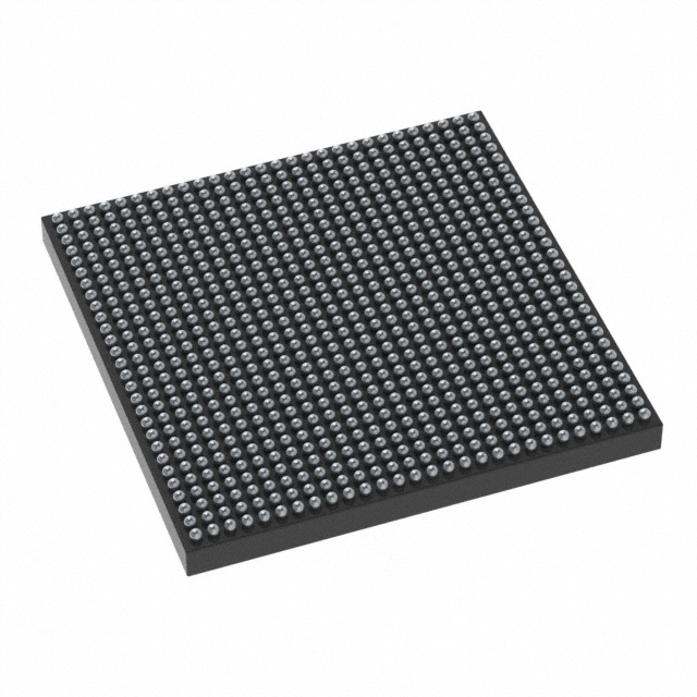
The XCKU9P-2FFVE900I is a Kintex® UltraScale+™ Field Programmable Gate Array (FPGA) IC configured in a 900‑ball FCBGA (31×31) package. It delivers a high-capacity programmable fabric with a combination of logic resources, embedded memory, and I/O suitable for complex digital designs.
With approximately 599,550 logic elements, roughly 41.88 Mbits of embedded memory and 304 I/O, this device targets designs that require significant on-chip logic and memory density while operating across an industrial temperature range.
Key Features
- Core Logic Approximately 599,550 logic elements and about 34,260 configurable logic blocks (CLBs) provide the programmable fabric for large-scale digital implementations.
- Embedded Memory Approximately 41.88 Mbits of on-chip RAM support large data buffers, state storage, and memory-intensive processing without relying solely on external memory.
- I/O Capacity 304 user I/O pins enable extensive interfacing and high-density connectivity for multiple peripherals and parallel busses.
- Package Supplied in a 900‑ball FCBGA (31×31) package for high-density board integration and surface-mount assembly.
- Power Supply Core voltage supply range of 825 mV to 876 mV for precise power-domain planning and integration into regulated power systems.
- Thermal and Reliability Rated for operation from −40 °C to 100 °C and specified as Industrial grade to support deployments in demanding environments.
- Mounting and Compliance Surface-mount device construction and RoHS compliance for modern assembly and regulatory needs.
Typical Applications
- High-performance digital signal processing — Use the large logic capacity and substantial embedded memory to implement complex signal chains and buffering on-chip.
- Compute and acceleration modules — Leverage the high logic element count and abundant I/O for custom compute kernels and data movement paths.
- Industrial control and automation — Industrial temperature rating and robust I/O count make the device suitable for demanding control, monitoring, and interface functions.
- Prototype and system integration — High-density programmable fabric supports consolidation of multiple functions for proof-of-concept and system validation.
Unique Advantages
- High logic density: Approximately 599,550 logic elements enable integration of complex state machines, controllers, and custom datapaths on a single device.
- Significant on-chip memory: Around 41.88 Mbits of embedded RAM reduce external memory dependence and simplify board-level memory architecture.
- Ample I/O count: 304 I/O pins support a wide range of interfaces and parallel connectivity options without immediate need for external expansion.
- Industrial operating range: Specified −40 °C to 100 °C supports reliable operation in temperature-demanding environments.
- Compact, high-density package: 900‑ball FCBGA (31×31) offers a space-efficient footprint for high-performance designs.
- Predictable core power window: Narrow voltage supply range (825–876 mV) aids precise power-supply design and domain control.
Why Choose XCKU9P-2FFVE900I?
The XCKU9P-2FFVE900I positions itself as a high-capacity FPGA solution that balances extensive programmable logic, substantial embedded memory, and a broad I/O complement within a compact FCBGA package. Its industrial temperature rating and RoHS compliance make it suitable for applications that require both performance and reliability.
This device is well suited for engineering teams and procurement focused on designs that demand on-chip resources for complex processing, dense interfacing, or consolidation of multiple functions onto a single programmable device. The combination of logic density, embedded RAM, and package density provides a scalable platform for medium- to large‑scale FPGA designs.
Request a quote or submit a quotation request for the XCKU9P-2FFVE900I to receive pricing and availability information tailored to your project needs.






















Date Founded: 1969
Headquarters: Santa Clara, California, USA
Employees: 25,000+
Revenue: $22.68 Billion
Certifications and Memberships: ISO9001:2015, RoHS, REACH











