
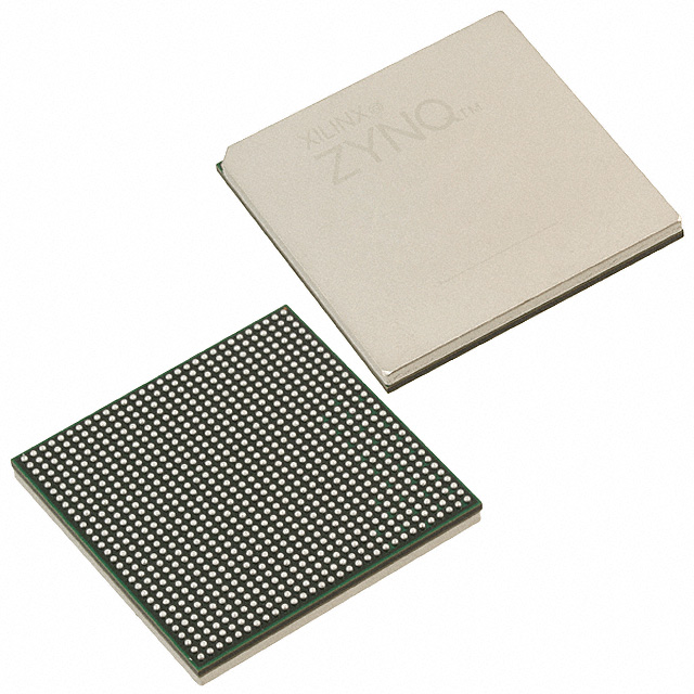
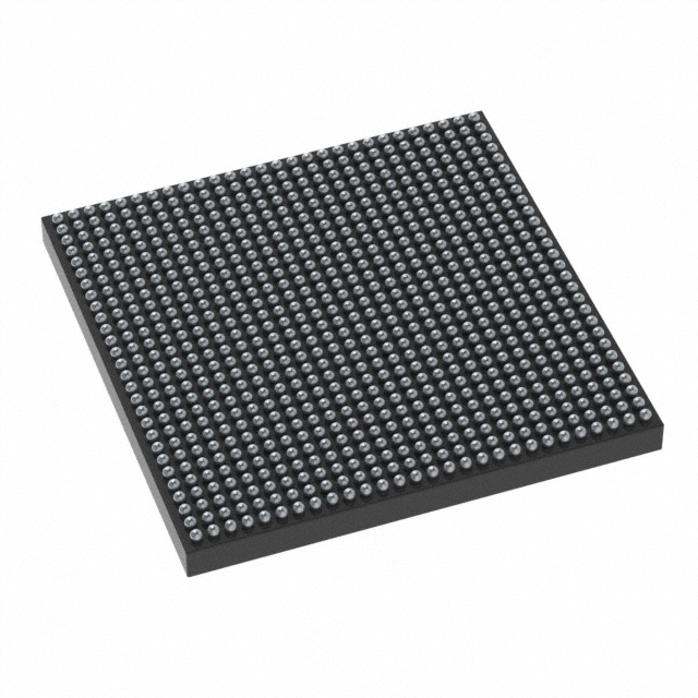
XCKU9P-2FFVE900E
| Part Description |
Kintex® UltraScale+™ Field Programmable Gate Array (FPGA) IC 304 41881600 599550 900-BBGA, FCBGA |
|---|---|
| Quantity | 597 Available (as of June 15, 2026) |

| Product Category | Field Programmable Gate Array (FPGA) |
|---|---|
| Manufacturer | AMD |
| Manufacturing Status | Active |
| Manufacturer Standard Lead Time | 16 Weeks |
| Datasheet |
Specifications & Environmental
| Device Package | 900-FCBGA (31x31) | Grade | Extended | Operating Temperature | 0°C – 100°C | ||
|---|---|---|---|---|---|---|---|
| Package / Case | 900-BBGA, FCBGA | Number of I/O | 304 | Voltage | 825 mV - 876 mV | ||
| Mounting Method | Surface Mount | RoHS Compliance | ROHS3 Compliant | REACH Compliance | REACH Unknown | ||
| Moisture Sensitivity Level | 4 (72 Hours) | Number of LABs/CLBs | 34260 | Number of Logic Elements/Cells | 599550 | ||
| Number of Gates | N/A | ECCN | 3A991D | HTS Code | 8542.39.0001 | ||
| Qualification | N/A | Total RAM Bits | 41881600 |
Overview of XCKU9P-2FFVE900E – Kintex® UltraScale+™ FPGA, 900-FCBGA
The XCKU9P-2FFVE900E is a Kintex® UltraScale+™ Field Programmable Gate Array (FPGA) IC from AMD, supplied in a 900-FCBGA surface-mount package. It delivers high programmable logic capacity and substantial on-chip memory for complex digital designs.
Key hardware characteristics include 599,550 logic elements, approximately 41.9 Mbits of embedded memory, 304 user I/Os, and a defined supply voltage window of 825 mV to 876 mV, all packaged in a 900-FCBGA (31×31) form factor with an extended operating grade.
Key Features
- Core Logic 599,550 logic elements provide high-density programmable logic resources for large designs.
- Embedded Memory Total on-chip RAM equals 41,881,600 bits (approximately 41.9 Mbits) for local storage and buffering.
- I/O Resources 304 user I/O pins to support broad interfacing and parallel connectivity needs.
- Power Supply Defined voltage supply range from 825 mV to 876 mV for predictable power design and supply planning.
- Package & Mounting 900-FCBGA (31×31) / 900-BBGA package in a surface-mount configuration for compact board-level integration.
- Operating Range & Grade Extended grade device with an operating temperature range of 0 °C to 100 °C.
Unique Advantages
- High logic density: 599,550 logic elements consolidate complex functions into a single device, reducing multi-device BOM and board complexity.
- Significant embedded RAM: Approximately 41.9 Mbits of on-chip memory reduce dependence on external memory for many buffering and working-set requirements.
- Ample I/O count: 304 I/Os simplify system integration by providing numerous connections for peripherals, sensors, and board-level signals.
- Compact, high-pin package: The 900-FCBGA (31×31) package enables high-density PCB layouts while maintaining large I/O and logic capacity.
- predictable power requirements: A narrow supply voltage window (825–876 mV) supports precise power budgeting for system designers.
- Extended operating grade: Rated for 0 °C to 100 °C operation, suitable for a range of standard operating environments.
Why Choose XCKU9P-2FFVE900E?
The XCKU9P-2FFVE900E is positioned for designs that require a combination of very high programmable logic capacity, substantial embedded memory, and broad I/O capability in a compact FCBGA package. Its specified supply range and extended operating grade make it a predictable choice for boards optimized for performance and density.
This FPGA is suitable for engineering teams and procurement seeking a single-device solution that consolidates logic, memory, and I/O to simplify system design and reduce component count while maintaining explicit, verifiable hardware specifications.
Request a quote or submit an inquiry to receive pricing and availability information for the XCKU9P-2FFVE900E.


Date Founded: 1969
Headquarters: Santa Clara, California, USA
Employees: 25,000+
Revenue: $22.68 Billion
Certifications and Memberships: ISO9001:2015, RoHS, REACH


