
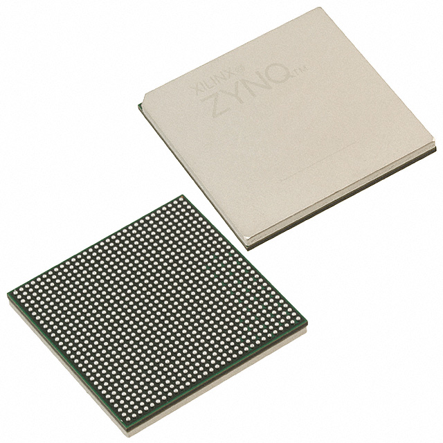
XCKU5P-L2SFVB784E
| Part Description |
Kintex® UltraScale+™ Field Programmable Gate Array (FPGA) IC 304 41984000 474600 784-BFBGA, FCBGA |
|---|---|
| Quantity | 988 Available (as of June 18, 2026) |

| Product Category | Field Programmable Gate Array (FPGA) |
|---|---|
| Manufacturer | AMD |
| Manufacturing Status | Active |
| Manufacturer Standard Lead Time | 16 Weeks |
| Datasheet |
Specifications & Environmental
| Device Package | 784-FCBGA (23x23) | Grade | Extended | Operating Temperature | 0°C – 110°C | ||
|---|---|---|---|---|---|---|---|
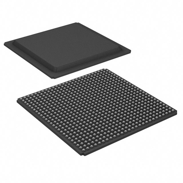
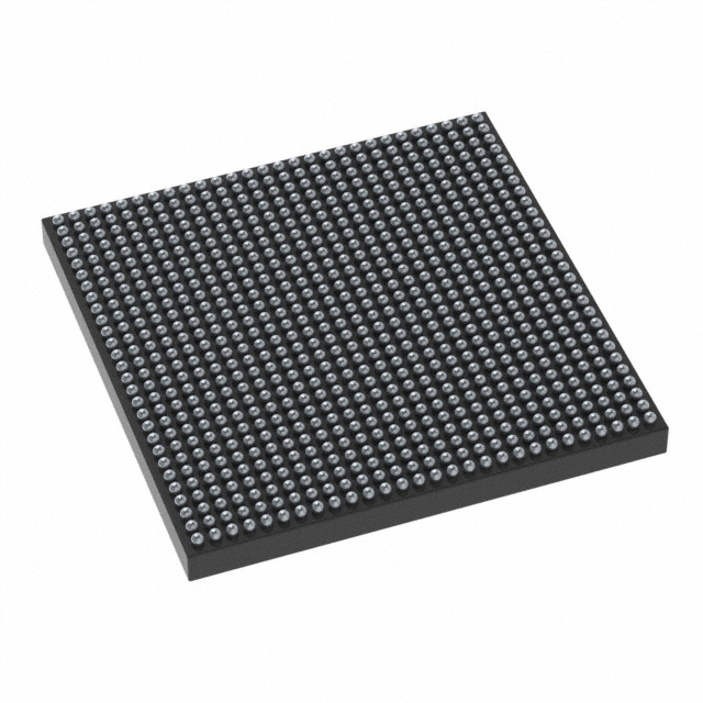
| Package / Case | 784-BFBGA, FCBGA | Number of I/O | 304 | Voltage | 698 mV - 876 mV | ||
| Mounting Method | Surface Mount | RoHS Compliance | ROHS3 Compliant | REACH Compliance | REACH Unknown | ||
| Moisture Sensitivity Level | 4 (72 Hours) | Number of LABs/CLBs | 27120 | Number of Logic Elements/Cells | 474600 | ||
| Number of Gates | N/A | ECCN | 3A991D | HTS Code | 8542.39.0001 | ||
| Qualification | N/A | Total RAM Bits | 41984000 |
Overview of XCKU5P-L2SFVB784E – Kintex® UltraScale+™ Field Programmable Gate Array, 784-FCBGA
The XCKU5P-L2SFVB784E is a Kintex® UltraScale+™ Field Programmable Gate Array (FPGA) manufactured by AMD. It provides a large programmable-logic resource set, significant on-chip RAM, and a high pin-count BGA package for complex embedded designs.
Key device metrics include 474,600 logic elements, approximately 42 Mbits of embedded memory, and 304 I/O pins. The device is supplied in a 784-FCBGA (23×23) package, supports a supply range of 698 mV to 876 mV, and is rated for an operating temperature range of 0°C to 110°C (Extended grade).
Key Features
- Logic Capacity — 474,600 logic elements provide the programmable fabric required for large-scale logic integration and complex algorithm implementation.
- Embedded Memory — Approximately 42 Mbits of on-chip RAM to support buffering, lookup tables, and embedded data storage without external memory for many functions.
- I/O Density — 304 user I/O pins enable extensive interfacing with peripherals, sensors, and external devices in high-density designs.
- Package — 784-BFBGA / 784-FCBGA (23×23) surface-mount package for high-pin-count board-level integration.
- Power — Operates across a supply range of 698 mV to 876 mV to match system power-rail requirements.
- Temperature & Grade — Extended-grade device rated for 0°C to 110°C operating temperature, suited for applications requiring beyond-commercial temperature range support.
- Mounting — Surface-mount package compatible with standard PCB assembly processes for BGA components.
Typical Applications
- High-capacity programmable logic — Use the device's 474,600 logic elements to implement large custom datapath, control logic, or protocol processing blocks.
- Embedded memory-centric designs — Approximately 42 Mbits of on-chip RAM can be applied to packet buffering, frame storage, or LUT-based processing without immediate dependence on external memory.
- High-pin-count system interfaces — 304 I/O pins enable connectivity to multiple high-speed interfaces, dense sensor arrays, or extensive peripheral sets.
- Board-level integration — The 784-FCBGA (23×23) surface-mount package supports compact, high-density PCB layouts for space-constrained applications.
Unique Advantages
- Large logic resource — 474,600 logic elements allow consolidation of multiple functions into a single FPGA, reducing component count and BOM complexity.
- Substantial on-chip memory — Approximately 42 Mbits of embedded RAM reduces dependence on external memory for many buffering and storage needs, improving system responsiveness.
- High I/O capacity — 304 I/Os enable flexible partitioning of signals and extensive peripheral connectivity without external multiplexing.
- Compact high-density package — The 784-FCBGA (23×23) package delivers high pin-count in a compact surface-mount form factor for modern PCB designs.
- Operational range — Extended-grade rating and 0°C to 110°C operating temperature support deployments that require wider-than-standard commercial temperature tolerance.
- Defined supply window — A specified supply range of 698 mV to 876 mV enables clear power-system design and sequencing considerations.
Why Choose XCKU5P-L2SFVB784E?
The XCKU5P-L2SFVB784E combines a very large logic fabric, significant on-chip memory, and high I/O count in a 784-FCBGA surface-mount package. Its extended-grade temperature rating and defined supply range make it a strong option for designs requiring substantial programmable resources and reliable operation across a broader temperature range.
This device is well suited for engineering teams targeting complex, integrated FPGA implementations where consolidation of logic and memory resources on-chip simplifies board-level design and helps manage system-level complexity.
Request a quote or submit an inquiry to obtain pricing and availability for the XCKU5P-L2SFVB784E. Our team can assist with lead time and ordering details.


Date Founded: 1969
Headquarters: Santa Clara, California, USA
Employees: 25,000+
Revenue: $22.68 Billion
Certifications and Memberships: ISO9001:2015, RoHS, REACH


