
XCKU9P-1FFVE900I
| Part Description |
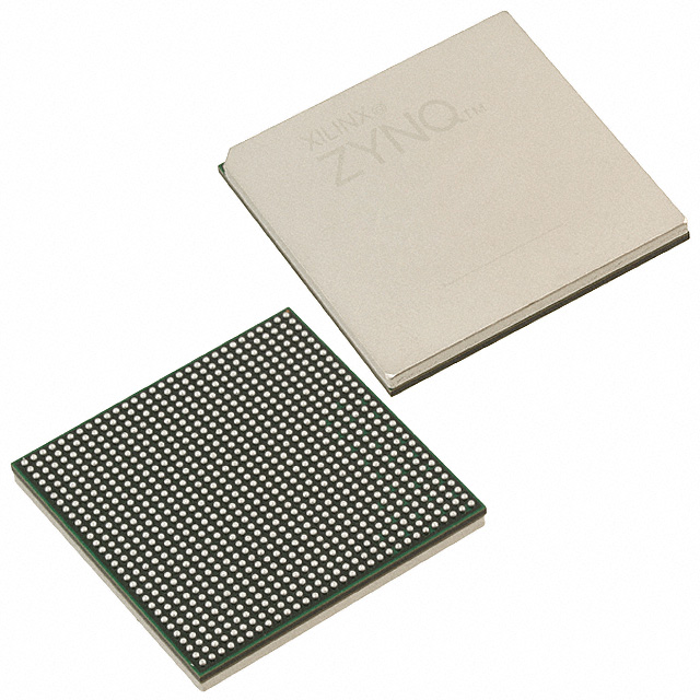
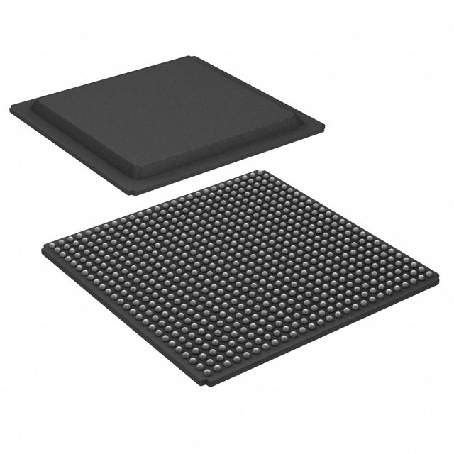
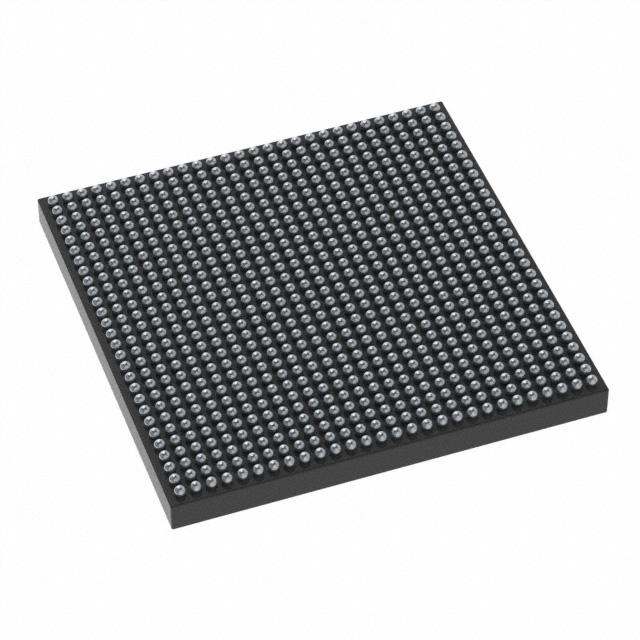
Kintex® UltraScale+™ Field Programmable Gate Array (FPGA) IC 304 41881600 599550 900-BBGA, FCBGA |
|---|---|
| Quantity | 1,691 Available (as of October 8, 2026) |

| Product Category | Field Programmable Gate Array (FPGA) |
|---|---|
| Manufacturer | AMD |
| Manufacturing Status | Active |
| Manufacturer Standard Lead Time | 16 Weeks |
| Datasheet |
Specifications & Environmental
| Device Package | 900-FCBGA (31x31) | Grade | Industrial | Operating Temperature | -40°C – 100°C | ||
|---|---|---|---|---|---|---|---|
| Package / Case | 900-BBGA, FCBGA | Number of I/O | 304 | Voltage | 825 mV - 876 mV | ||
| Mounting Method | Surface Mount | RoHS Compliance | ROHS3 Compliant | REACH Compliance | REACH Unknown | ||
| Moisture Sensitivity Level | 4 (72 Hours) | Number of LABs/CLBs | 34260 | Number of Logic Elements/Cells | 599550 | ||
| Number of Gates | N/A | ECCN | 3A991D | HTS Code | 8542.39.0001 | ||
| Qualification | N/A | Total RAM Bits | 41881600 |
Overview of XCKU9P-1FFVE900I – Kintex® UltraScale+™ FPGA, 599,550 logic elements, 900‑FCBGA
The XCKU9P-1FFVE900I is a Kintex® UltraScale+™ Field Programmable Gate Array (FPGA) IC from AMD, packaged in a 900‑ball FCBGA (31×31) format. It delivers a high logic element count and substantial on‑chip memory capacity in a surface‑mount industrial‑grade device.
With 599,550 logic elements, approximately 41.9 Mbits of embedded memory and 304 I/O pins, this device is designed for applications that require significant programmable logic, memory resources and flexible I/O in a compact package. The device operates over an industrial temperature range and supports a low core supply window for system power planning.
Key Features
- Logic Capacity — 599,550 logic elements and 34,260 configurable logic blocks (CLBs) provide large-scale programmable logic resources for complex designs.
- Embedded Memory — Approximately 41.9 Mbits of on‑chip RAM to support buffering, caching and logic‑local storage needs.
- I/O Resources — 304 user I/O pins for broad external device interfacing and system connectivity.
- Power — Core voltage supply range specified at 825 mV to 876 mV to guide power‑delivery design.
- Package and Mounting — 900‑BBGA, FCBGA package (900‑FCBGA, 31×31) in a surface‑mount form factor for compact board integration.
- Operating Environment — Industrial grade device with an operating temperature range of −40 °C to 100 °C for deployment in temperature‑challenging environments.
- RoHS Compliant — Conforms to RoHS environmental requirements.
Typical Applications
- Industrial Control and Automation — Implement deterministic logic, protocol bridging and real‑time data handling using the device’s large logic and memory resources.
- Communications Infrastructure — Use abundant I/O and programmable logic to implement interface processing, packet handling and protocol acceleration.
- Imaging and Video Processing — Leverage on‑chip memory and rich logic fabric for buffering, pixel processing and custom video pipelines.
- High‑Performance Embedded Systems — Integrate complex control and compute functions within a compact FCBGA package for space‑constrained boards.
Unique Advantages
- High Logic Density: 599,550 logic elements enable large, feature‑rich FPGA designs without board‑level partitioning.
- Substantial On‑Chip Memory: Approximately 41.9 Mbits of embedded RAM reduces reliance on external memory for many buffering and caching tasks.
- Extensive I/O Count: 304 I/O pins provide flexibility to connect multiple peripherals and high‑speed interfaces directly to the FPGA.
- Industrial Temperature Range: −40 °C to 100 °C rating supports deployment in a wide range of operational environments.
- Compact FCBGA Package: 900‑ball FCBGA (31×31) balances I/O density and board footprint for high‑density designs.
- Defined Power Envelope: Core supply specified between 825 mV and 876 mV to assist in precise power delivery and thermal planning.
Why Choose XCKU9P-1FFVE900I?
The XCKU9P-1FFVE900I positions itself as a scalable, industrial‑grade FPGA option for designs that demand high logic density, significant embedded memory and extensive I/O in a compact package. Its combination of 599,550 logic elements, roughly 41.9 Mbits of on‑chip RAM and 304 I/O pins supports complex, integrated system designs without excessive external components.
This device is suited to engineers and system designers building industrial automation, communications, imaging or high‑performance embedded systems who require predictable operating temperature margins, a defined core voltage window and a surface‑mount 900‑ball FCBGA footprint for board integration.
Request a quote or submit a parts inquiry to receive pricing, lead time and availability information for the XCKU9P-1FFVE900I. Our team can assist with ordering and provide the documentation you need to move your design forward.





















Date Founded: 1969
Headquarters: Santa Clara, California, USA
Employees: 25,000+
Revenue: $22.68 Billion
Certifications and Memberships: ISO9001:2015, RoHS, REACH











