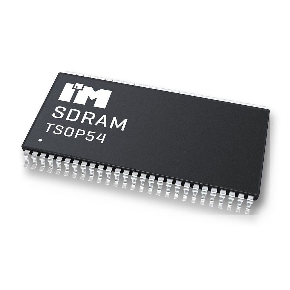
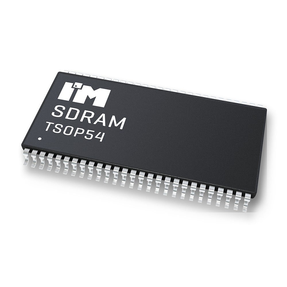
IM2508SDBBTG-6
| Part Description |
SDRAM, 256MB, 3.3V, 32MX8, 166MH |
|---|---|
| Quantity | 226 Available (as of June 15, 2026) |
| Product Category | Memory |
|---|---|
| Manufacturer | Intelligent Memory Ltd. |
| Manufacturing Status | Active |
| Manufacturer Standard Lead Time | 8 Weeks |
| Datasheet |
Specifications & Environmental
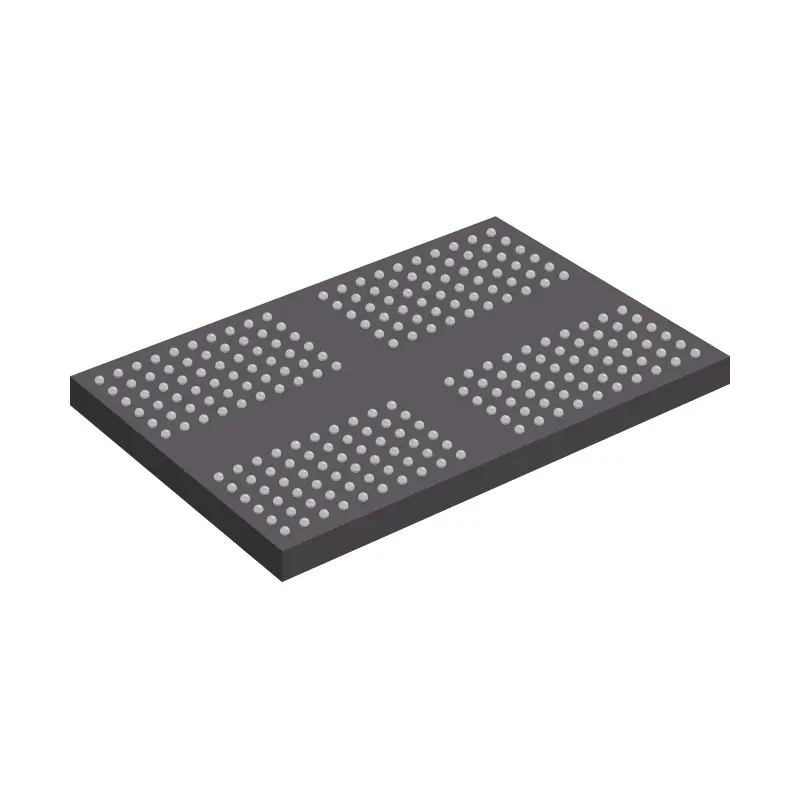
| Device Package | 54-TSOP II | Memory Format | DRAM | Technology | SDRAM | ||
|---|---|---|---|---|---|---|---|
| Memory Size | 256 Mbit | Access Time | 5.4 ns | Grade | Commercial | ||
| Clock Frequency | 166 MHz | Voltage | 3V ~ 3.6V | Memory Type | Volatile | ||
| Operating Temperature | 0°C ~ 70°C (TA) | Write Cycle Time Word Page | 15 ns | Packaging | 54-TSOP (0.400", 10.16mm Width) | ||
| Mounting Method | Volatile | Memory Interface | LVTTL | Memory Organization | 32M x 8 | ||
| Moisture Sensitivity Level | 3 (168 Hours) | RoHS Compliance | ROHS3 Compliant | REACH Compliance | REACH Affected | ||
| Qualification | N/A | ECCN | EAR99 | HTS Code | 8542.32.0024 |
Overview of IM2508SDBBTG-6 – 256Mbit SDRAM, 3.3V, 32M×8, 166MHz
The IM2508SDBBTG-6 is a 256Mbit synchronous DRAM organized as 4 banks × 8Mbit × 8, operating from a 3.3 V supply. It delivers high-speed, fully synchronous memory operation with outputs synchronized to the rising edge of an external clock and supports clock frequencies up to 166 MHz (PC166).
Designed for systems that require predictable, clocked DRAM behavior, the device supports programmable CAS latency, multiple burst lengths and bank interleaving to enable efficient sequential and random access patterns while providing standard LVTTL I/O signaling.
Key Features
- Core Architecture Four-bank organization (4 banks × 8Mbit × 8) enabling interleaved operation and improved random-access throughput.
- Performance Supports system clock frequencies up to 166 MHz with clock access time tAC = 5.4 ns (CAS latency = 3); programmable CAS latency 2 or 3.
- Memory Capacity & Organization 256 Mbit total capacity arranged as 32M × 8, with programmable burst lengths of 1, 2, 4, 8 and full-page (sequential) or 1, 2, 4, 8 (interleave).
- Interfaces & Control LVTTL I/O interface with standard synchronous control signals (CLK, CKE, CS, RAS, CAS, WE, BA0/BA1, A0–A12) and data mask (DQM) for read/write control.
- Power & Refresh Single 3.3 V ±0.3 V supply (operating range 3.0 V–3.6 V) with power-down mode, auto-refresh and self-refresh support; refresh interval 8192 cycles per 64 ms.
- Timing & Reliability Typical access time 5.4 ns, write cycle time (word/page) 15 ns, and support for single-pulsed RAS and automatic/controlled precharge operations.
- Package & Environmental Available in a 54-pin TSOP II package (0.400" / 10.16 mm width); commercial operating temperature 0°C to 70°C TA.
Typical Applications
- High-speed system memory Use as synchronous DRAM in designs that require clocked memory operation up to 166 MHz and programmable CAS latency.
- Burst and sequential data buffering Programmable burst lengths and sequential/interleave options enable efficient burst reads and writes for data streaming and buffering tasks.
- 3.3 V embedded memory expansion 256 Mbit density in a 54-pin TSOP II package provides compact on-board memory for 3.3 V systems.
Unique Advantages
- Programmable CAS latency: CL selectable between 2 and 3 to match system timing and balance latency versus stability.
- Flexible burst control: Multiple burst lengths and sequential/interleave wrap modes simplify tuning for sequential data throughput or random-access efficiency.
- Bank interleaving: Four independent banks (BA0/BA1) allow interleaved operation to increase effective random access rate.
- Standard LVTTL interface: LVTTL signaling for control and I/O supports straightforward integration with LVTTL-compatible system logic.
- Integrated power management: Power-down, auto-refresh and self-refresh modes reduce system-level refresh management complexity.
- Compact, industry-standard package: 54-pin TSOP II provides a space-efficient footprint for board-level memory implementations.
Why Choose IM2508SDBBTG-6?
The IM2508SDBBTG-6 combines a 256 Mbit density and a four-bank synchronous DRAM architecture with programmable latency and burst controls to deliver deterministic, clock-synchronous memory behavior at up to 166 MHz. Its LVTTL interface, integrated refresh modes and standard TSOP II packaging make it suitable for designers looking for a predictable, board-level SDRAM solution in 3.3 V systems.
This part is appropriate for projects that require configurable latency, burst-oriented transfers and bank-interleaved access patterns while operating within a commercial temperature range. Its fixed electrical and timing characteristics simplify system timing integration and support straightforward memory expansion on constrained PCBs.
To request a quote or obtain availability and pricing details for the IM2508SDBBTG-6, submit an inquiry and include your target quantities and lead-time requirements.