IM2516SDBDBG-6I
| Part Description |
SDRAM, 256MB, 3.3V, 16MX16, 166M |
|---|---|
| Quantity | 1,494 Available (as of June 9, 2026) |

| Product Category | Memory |
|---|---|
| Manufacturer | Intelligent Memory Ltd. |
| Manufacturing Status | Active |
| Manufacturer Standard Lead Time | 8 Weeks |
| Datasheet |
Specifications & Environmental
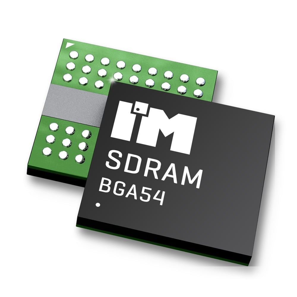
| Device Package | 54-FBGA (8x8) | Memory Format | DRAM | Technology | SDRAM | ||
|---|---|---|---|---|---|---|---|
| Memory Size | 256 Mbit | Access Time | 5 ns | Grade | Automotive | ||
| Clock Frequency | 166 MHz | Voltage | 3V ~ 3.6V | Memory Type | Volatile | ||
| Operating Temperature | -40°C ~ 95°C (TC) | Write Cycle Time Word Page | 12 ns | Packaging | 54-TFBGA | ||
| Mounting Method | Volatile | Memory Interface | LVTTL | Memory Organization | 16M x 16 | ||
| Moisture Sensitivity Level | 3 (168 Hours) | RoHS Compliance | ROHS3 Compliant | REACH Compliance | REACH Affected | ||
| Qualification | N/A | ECCN | EAR99 | HTS Code | 8542.32.0024 |
Overview of IM2516SDBDBG-6I – 256Mbit SDRAM, 3.3 V, 16M × 16, 166 MHz
The IM2516SDBDBG-6I is a synchronous DRAM device organized as 4 banks × 4Mbit × 16, delivering 256 Mbit of volatile memory in a high‑speed, pipelined architecture. The device supports full synchronous operation with LVTTL I/O and is specified for operation with a single 3.3 V ±0.3 V supply.
Designed for systems that require predictable, clock‑aligned memory access, the IM2516SDBDBG-6I provides programmable CAS latency and burst options to match a range of timing and throughput requirements, and is available in a compact 54‑ball FBGA package.
Key Features
- Core Organization — 4 banks × 4Mbit × 16 organization (16M × 16 overall) providing 256 Mbit of SDRAM storage.
- Performance — Supports clock rates up to 166 MHz with an access time from CLK up to 5 ns and clock cycle time of 6 ns (ordering speed code -6).
- Programmable Timing and Burst — Programmable CAS latency options (2, 3), selectable burst type (Sequential or Interleaved) and burst lengths of 1, 2, 4, 8 or full page; burst stop function supported.
- Refresh and Power Management — Auto Refresh and Self Refresh supported with 8192 refresh cycles/64 ms; CKE power‑down mode available for reduced power during idle periods.
- Interface and Signaling — LVTTL interface for data and control signals; all control, address and data I/O synchronized to the positive edge of the external clock.
- Voltage — Single supply: 3.3 V ±0.3 V (specified 3.0 V to 3.6 V).
- Timing Parameters — Write cycle time (word/page) 12 ns; row active time (tRAS) min. 42 ns; row cycle time (tRC) min. 60 ns.
- Package — Available in 54‑ball FBGA (8 mm × 8 mm) and 54‑pin TSOP II; supplier device package listed as 54‑FBGA (8×8).
- Operating Temperature Options — Datasheet options include Commercial (0°C to +70°C) and Industrial (−40°C to +85°C) ambient temperature ranges.
- I/O Characteristics — Input capacitance 2–4 pF; input/output capacitance 4–6 pF (typical conditions per datasheet).
Typical Applications
- Embedded memory subsystems — Use as synchronous main or buffer memory where 256 Mbit SDRAM with LVTTL signaling and clocked operation is required.
- High‑throughput data buffering — Burst modes, programmable CAS latency and pipelined architecture support sequential or interleaved high‑speed transfers up to 166 MHz.
- Industrial temperature systems — Industrial temperature option (−40°C to +85°C) supports deployment in thermally demanding environments.
Unique Advantages
- Configurable latency and burst behavior: Programmable CAS latency (2 or 3) and selectable burst lengths allow designers to tune latency and throughput to system requirements.
- Synchronous, pipelined architecture: Full synchronous operation and internal pipelining synchronize control, address and data to an external clock for deterministic timing.
- Standardized LVTTL interface: LVTTL signaling simplifies integration with logic level systems that use 3.3 V interfaces.
- Compact BGA footprint: 54‑ball FBGA (8 mm × 8 mm) package reduces board area for designs with tight space constraints.
- Built‑in refresh and low‑power modes: Auto Refresh, Self Refresh and CKE power‑down support system power management and data retention during idle periods.
- Industry temperature option: Availability of industrial temperature grading supports deployment across a wider ambient temperature range.
Why Choose SDRAM, 256MB, 3.3V, 16MX16, 166M?
The IM2516SDBDBG-6I is positioned for designs that need a synchronous, high‑speed DRAM with flexible timing options and industry‑grade operating ranges. Its 4‑bank architecture, programmable CAS latency, and burst configurations provide tuning options for a variety of throughput and latency tradeoffs.
This device is suited to engineers specifying a 256 Mbit SDRAM with LVTTL I/O and compact FBGA packaging where predictable, clocked memory behavior and standard refresh/power modes are required. The datasheet‑defined timing, supply, and temperature options provide a clear basis for system integration and long‑term deployment planning.
Request a quote or submit a pricing inquiry for IM2516SDBDBG-6I to obtain availability, lead times and volume pricing information.