IM6416SDBABG-6I
| Part Description |
SDRAM, 64MB, 3.3V, 4MX16, 166MHZ |
|---|---|
| Quantity | 1,003 Available (as of June 15, 2026) |
| Product Category | DRAM Memory |
|---|---|
| Manufacturer | Intelligent Memory Ltd. |
| Manufacturing Status | Active |
| Manufacturer Standard Lead Time | 8 Weeks |
| Datasheet |
Specifications & Environmental
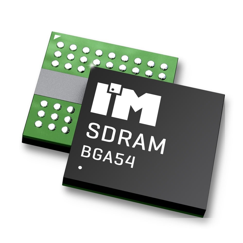
| Device Package | 54-FBGA (8x8) | Memory Format | DRAM | Technology | SDRAM | ||
|---|---|---|---|---|---|---|---|
| Memory Size | 64 Mbit | Access Time | 5.4 ns | Grade | Automotive | ||
| Clock Frequency | 166 MHz | Voltage | 3V ~ 3.6V | Memory Type | Volatile | ||
| Operating Temperature | -40°C ~ 95°C (TC) | Write Cycle Time Word Page | 2 ns | Packaging | 54-TFBGA | ||
| Mounting Method | Volatile | Memory Interface | LVTTL | Memory Organization | 4M x 16 | ||
| Moisture Sensitivity Level | 3 (168 Hours) | RoHS Compliance | ROHS Compliant | REACH Compliance | REACH Affected | ||
| Qualification | N/A | ECCN | EAR99 | HTS Code | 8542.32.0002 |
Overview of IM6416SDBABG-6I – SDRAM, 64MB, 3.3V, 4MX16, 166MHZ
The IM6416SDBABG-6I is a synchronous DRAM device organized as four banks × 1Mbit × 16, delivering a 64Mbit memory array with high-speed transfer capability up to 166 MHz. It implements full synchronous operation with all control, address and data signals referenced to the rising edge of an external clock.
Designed for systems that require programmable latency, burst transfers and bank interleave, the device supports a single 3.3 V ± 0.3 V supply (3.0 V–3.6 V), an LVTTL interface and is supplied in a 54-pin FBGA (8 mm × 8 mm) package with an extended operating temperature range.
Key Features
- Memory core — 4 banks × 1Mbit × 16 organization providing a total 64Mbit SDRAM array.
- Performance — Supports system frequencies up to 166 MHz with clock access times as low as 5.4 ns (CL = 3) and a clock cycle time of 6 ns at the -6 speed grade.
- Programmable burst and latency — Programmable CAS latency of 2 or 3 and selectable burst lengths (1, 2, 4, 8 and full page for sequential; 1, 2, 4, 8 for interleave) to match system throughput and access patterns.
- Synchronous command set — Full synchronous DRAM with single-pulsed RAS, data mask for read/write control, automatic and controlled precharge, and random column address every CLK (1-N rule).
- Refresh and low-power modes — Auto refresh and self refresh supported with a refresh interval of 4096 cycles/64 ms, plus a Power Down mode to reduce standby current.
- Interface and supply — LVTTL I/O interface and single-supply operation from 3.0 V to 3.6 V (nominal 3.3 V).
- Package and thermal — Supplied in a 54-TFBGA (54-FBGA, 8 mm × 8 mm) package; specified operating temperature range −40 °C to 95 °C (TC) as provided in the product specification.
- Manufacturing and compliance — Lead-free / RoHS indicated in the device datasheet.
Typical Applications
- High-speed buffer memory — Use where synchronous burst transfers and interleaved bank access are required to sustain sequential data rates.
- Embedded system SDRAM — Suitable for designs needing a compact 64Mbit DRAM in a 54-ball FBGA package with programmable latency and burst control.
- Memory expansion for controllers — Fits applications that leverage LVTTL interfacing and single 3.3 V supply for external working RAM.
Unique Advantages
- Configurable latency and burst: Programmable CAS latency (2 or 3) and multiple burst length options let designers balance access latency against sustained throughput.
- Interleaved bank architecture: Four-bank organization enables higher random access rates via interleaving, improving effective throughput for mixed access patterns.
- Compact BGA package: The 54-FBGA (8 mm × 8 mm) footprint provides a small form factor for space-constrained boards while maintaining full 16-bit data width.
- Comprehensive refresh and power modes: Auto/self refresh and Power Down reduce system management overhead and help control standby power.
- Synchronous timing for system integration: All control, address and data signals referenced to clock rising edge simplify timing closure in synchronous designs.
Why Choose SDRAM, 64MB, 3.3V, 4MX16, 166MHZ?
The IM6416SDBABG-6I combines a compact FBGA package with a 4-bank, 16-bit SDRAM architecture and up to 166 MHz operation, making it a practical choice for designs that require configurable burst behavior and synchronous timing. Its LVTTL interface, single-supply 3.0 V–3.6 V operation and supported low-power refresh modes provide straightforward integration into a wide range of embedded systems.
This device is suited for engineers and procurement teams seeking a verified 64Mbit SDRAM offering programmable latency, robust refresh control and a small footprint package for scalable, space-efficient memory implementations.
Request a quote or submit a pricing inquiry to receive availability and lead-time information for the IM6416SDBABG-6I.