IM5116D2DDBG-25
| Part Description |
DDR2 512MB, 1.8V, 32MX16, 400MHZ |
|---|---|
| Quantity | 609 Available (as of June 14, 2026) |
| Product Category | Memory |
|---|---|
| Manufacturer | Intelligent Memory Ltd. |
| Manufacturing Status | Active |
| Manufacturer Standard Lead Time | 8 Weeks |
| Datasheet |
Specifications & Environmental
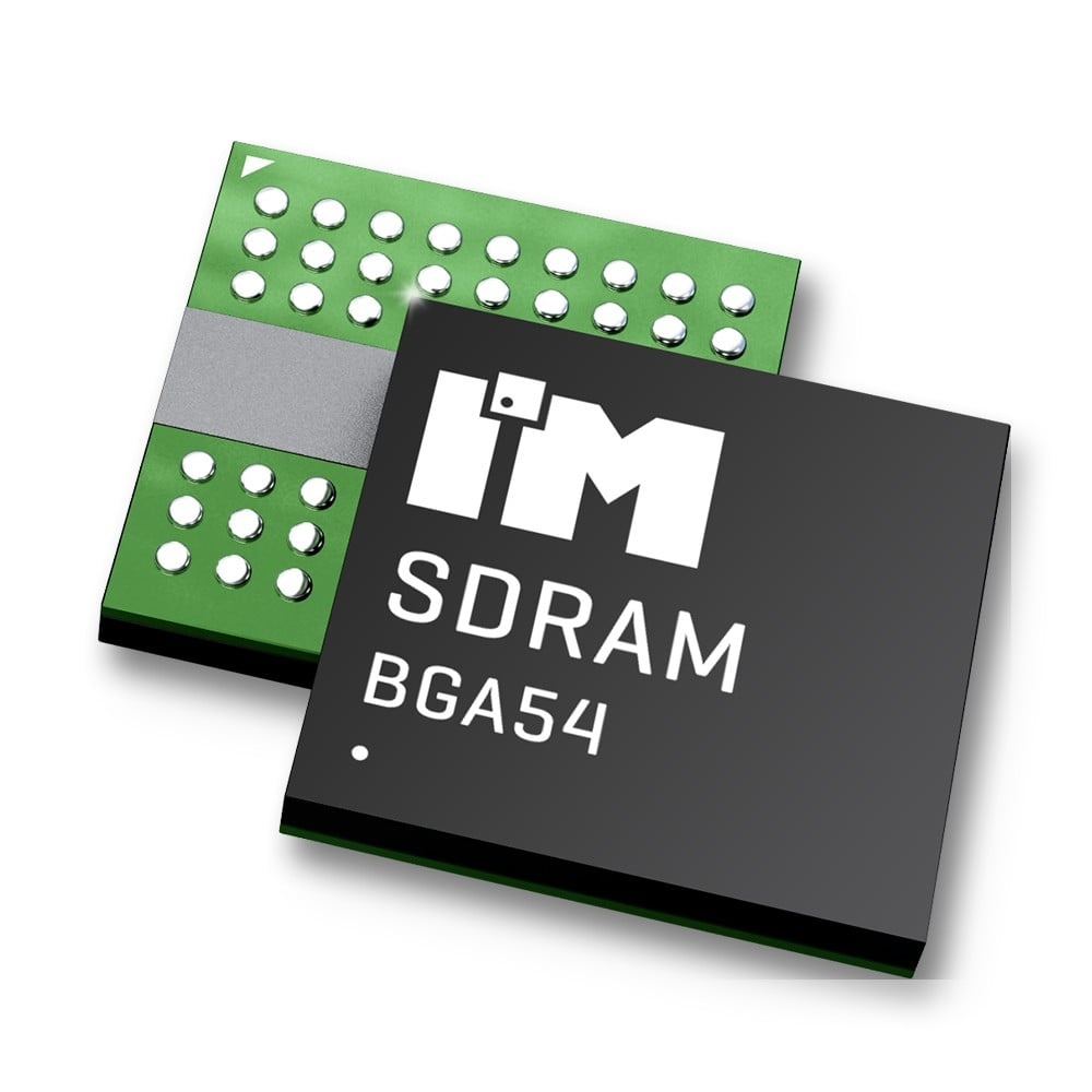
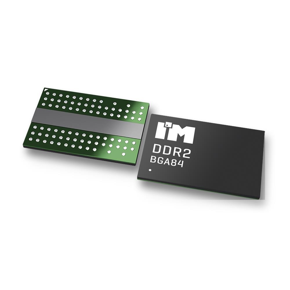
| Device Package | 84-FBGA (8x12.5) | Memory Format | DRAM | Technology | SDRAM - DDR2 | ||
|---|---|---|---|---|---|---|---|
| Memory Size | 512 Mbit | Access Time | 400 ps | Grade | Extended / Automotive-like | ||
| Clock Frequency | 400 MHz | Voltage | 1.7V ~ 1.9V | Memory Type | Volatile | ||
| Operating Temperature | 0°C ~ 95°C (TC) | Write Cycle Time Word Page | 15 ns | Packaging | 84-TFBGA | ||
| Mounting Method | Volatile | Memory Interface | SSTL_18 | Memory Organization | 32M x 16 | ||
| Moisture Sensitivity Level | 3 (168 Hours) | RoHS Compliance | ROHS3 Compliant | REACH Compliance | REACH Affected | ||
| Qualification | N/A | ECCN | EAR99 | HTS Code | 8542.32.0028 |
Overview of IM5116D2DDBG-25 – DDR2 512MB, 1.8V, 32M×16, 400MHz
The IM5116D2DDBG-25 is a 512 Mbit DDR2 SDRAM organized as 32M × 16, optimized for 1.8 V SSTL_18 systems. It is the x16 component in Intelligent Memory’s IM51 DDR2 family and is offered in the -25 speed grade (DDR2-800 timing) with a 400 MHz system clock capability.
Designed for high-throughput memory applications, the device implements a 4-bank architecture, on-chip DLL and On-Die Termination to support synchronized, reliable DDR2 transfers while offering programmable latencies and refresh modes for system integration flexibility.
Key Features
- Memory Architecture 512 Mbit DDR2 SDRAM organized as 32M × 16 with 4 internal banks and a 4-bit prefetch architecture for burst transfers.
- Performance -25 speed grade (DDR2-800 timing) supporting a system clock frequency up to 400 MHz and an access time listed as 400 ps.
- Timing and Latency Programmable CAS latency settings (3, 4, 5, 6, 7) and programmable additive latency (0–6). Write latency equals read latency minus one.
- Burst, Wrap and Commands Programmable burst lengths of 4 or 8 and selectable wrap sequence (sequential or interleave). Supports automatic and controlled precharge commands.
- Power and Refresh JEDEC 1.8 V ±0.1 V supply (VDD and VDDQ), power-down mode, auto-refresh and self-refresh. Average refresh intervals: 7.8 µs (0°C ≤ Tcase ≤ 85°C) and 3.9 µs (85°C ≤ Tcase ≤ 95°C).
- Signal Integrity On-Die Termination (ODT), on-chip DLL to align DQ/DQs transitions with CK, and an option for weak-strength data-output drivers. Bidirectional differential data strobe (DQS/DQS) supported; single-ended DQS is optional.
- Interface SSTL_18 compatible memory interface for DDR2 system integration.
- Package and Temperature 84-ball FBGA (8 mm × 12.5 mm) package for the x16 component and a commercial case operating range of 0°C to 95°C.
- Operational Timing Write cycle time (word page) specified at 15 ns to support sustained write operations.
Unique Advantages
- DDR2-800 (–25) timing with 400 MHz system clock: Enables high-rate DDR2 transfers consistent with the -25 speed grade.
- Flexible latency programming: Multiple CAS and additive latency options let designers balance throughput and timing margins for target systems.
- On-chip timing and termination: DLL and ODT features improve signal alignment and termination without external components, aiding timing closure on DDR2 designs.
- Compact BGA footprint: 84-ball FBGA (8 × 12.5 mm) x16 package provides a space-efficient memory option for board-level integration.
- Commercial temperature range: Specified 0°C to 95°C Tcase for deployment in standard commercial environments.
Why Choose IM5116D2DDBG-25?
The IM5116D2DDBG-25 provides a verified DDR2 x16 memory option with DDR2-800 timing, programmable latency, and on-die features (ODT, DLL) that simplify timing and signal integrity management in DDR2 systems. Its SSTL_18 interface, 84-ball FBGA package, and commercial temperature rating make it suitable for system designs requiring a compact, configurable 512 Mbit DDR2 solution.
This device is appropriate for design teams focused on robust DDR2 memory integration where configurable timing, on-chip termination, and a compact package are required to meet board-level constraints and performance targets.
Request a quote or submit an inquiry to obtain pricing, availability and additional product support information for the IM5116D2DDBG-25.