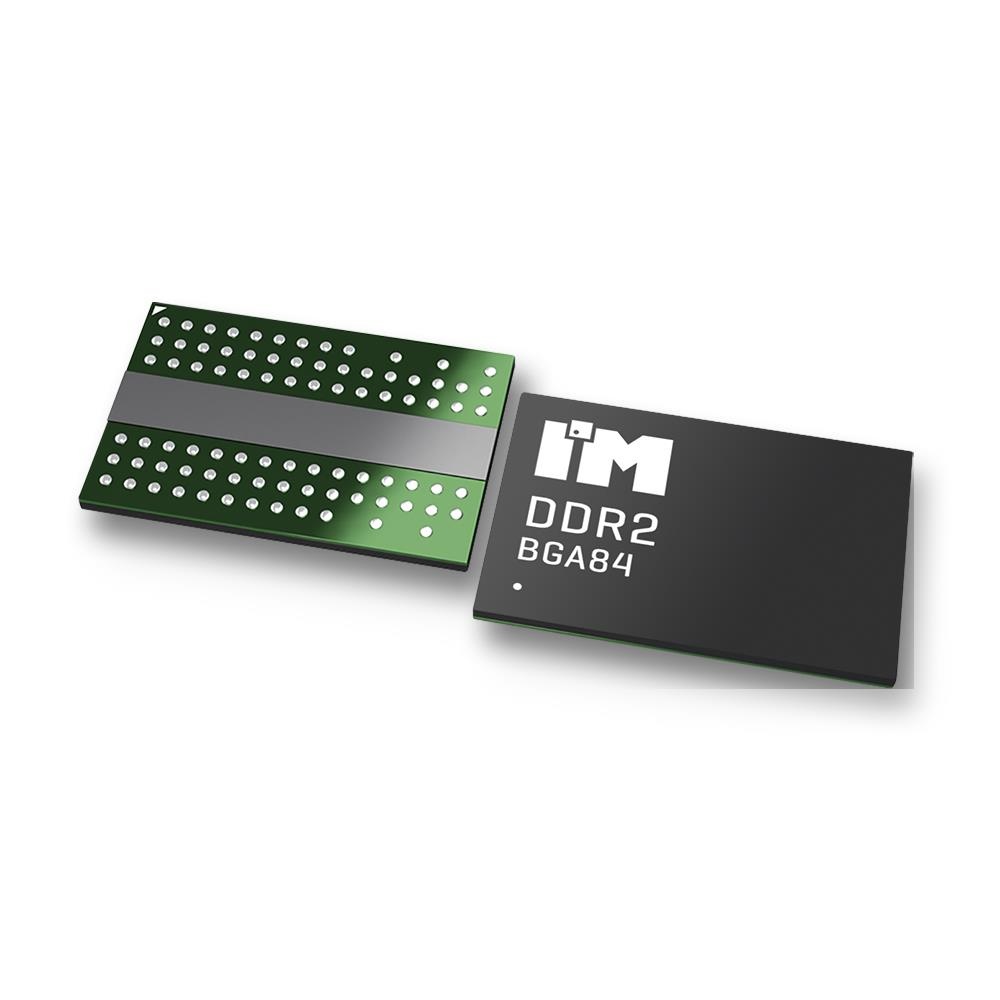
IM5116D2DDBG-25I
| Part Description |
DDR2 512MB, 1.8V, 32MX16, 400MHZ |
|---|---|
| Quantity | 863 Available (as of June 15, 2026) |

| Product Category | DRAM Memory |
|---|---|
| Manufacturer | Intelligent Memory Ltd. |
| Manufacturing Status | Active |
| Manufacturer Standard Lead Time | 8 Weeks |
| Datasheet |
Specifications & Environmental
| Device Package | 84-FBGA (8x12.5) | Memory Format | DRAM | Technology | SDRAM - DDR2 | ||
|---|---|---|---|---|---|---|---|
| Memory Size | 512 Mbit | Access Time | 400 ps | Grade | Automotive | ||
| Clock Frequency | 400 MHz | Voltage | 1.7V ~ 1.9V | Memory Type | Volatile | ||
| Operating Temperature | -40°C ~ 95°C (TC) | Write Cycle Time Word Page | 15 ns | Packaging | 84-TFBGA | ||
| Mounting Method | Volatile | Memory Interface | SSTL_18 | Memory Organization | 32M x 16 | ||
| Moisture Sensitivity Level | 3 (168 Hours) | RoHS Compliance | ROHS3 Compliant | REACH Compliance | REACH Affected | ||
| Qualification | N/A | ECCN | EAR99 | HTS Code | 8542.32.0028 |
Overview of IM5116D2DDBG-25I – DDR2 512MB, 1.8V, 32MX16, 400MHZ
The IM5116D2DDBG-25I is a DDR2 SDRAM device organized as 32M × 16 with a 512Mbit density and a 400 MHz clock rating. It implements a 4-bank architecture with 4-bit prefetch and on-chip DLL to synchronize data I/O to an external clock for high-speed system memory applications.
This device is specified for 1.7 V to 1.9 V supply operation and supports industrial case temperatures (–40°C to 95°C), making it suitable for systems that require 1.8 V DDR2 memory with programmable latency and on-die termination options.
Key Features
- Core & architecture Four internal banks with a 4-bit prefetch architecture enable interleaved and concurrent operation across banks for efficient random and sequential access patterns.
- Memory organization & density Organized as 32M × 16 delivering 512 Mbit of DDR2 SDRAM capacity.
- Performance Rated for a system clock frequency up to 400 MHz (DDR2-800, speed code -25) with programmable CAS latencies of 3, 4, 5, 6 and 7 and programmable additive latency options.
- Timing & refresh Supports Auto Refresh and Self Refresh with typical refresh intervals of 7.8 μs (0°C to 85°C) and 3.9 μs (85°C to 95°C); write cycle time (word page) is specified at 15 ns and access time at 400 ps.
- Power & I/O JEDEC nominal supply and I/O (VDD/VDDQ) around 1.8 V (operating range 1.7 V to 1.9 V) and SSTL_18 memory interface signaling.
- On-die features On-Die Termination (ODT), optional weak-strength data-output driver, bidirectional differential data strobe (DQS/DQS), and an on-chip DLL for DQ/DQS alignment.
- Programmed behavior Programmable burst length (4 or 8), programmable wrap sequence (sequential or interleave), write latency = read latency − 1, and PASR (Partial Array Self Refresh) support.
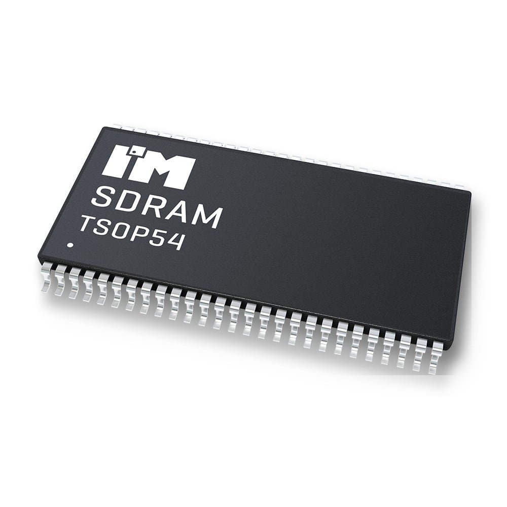
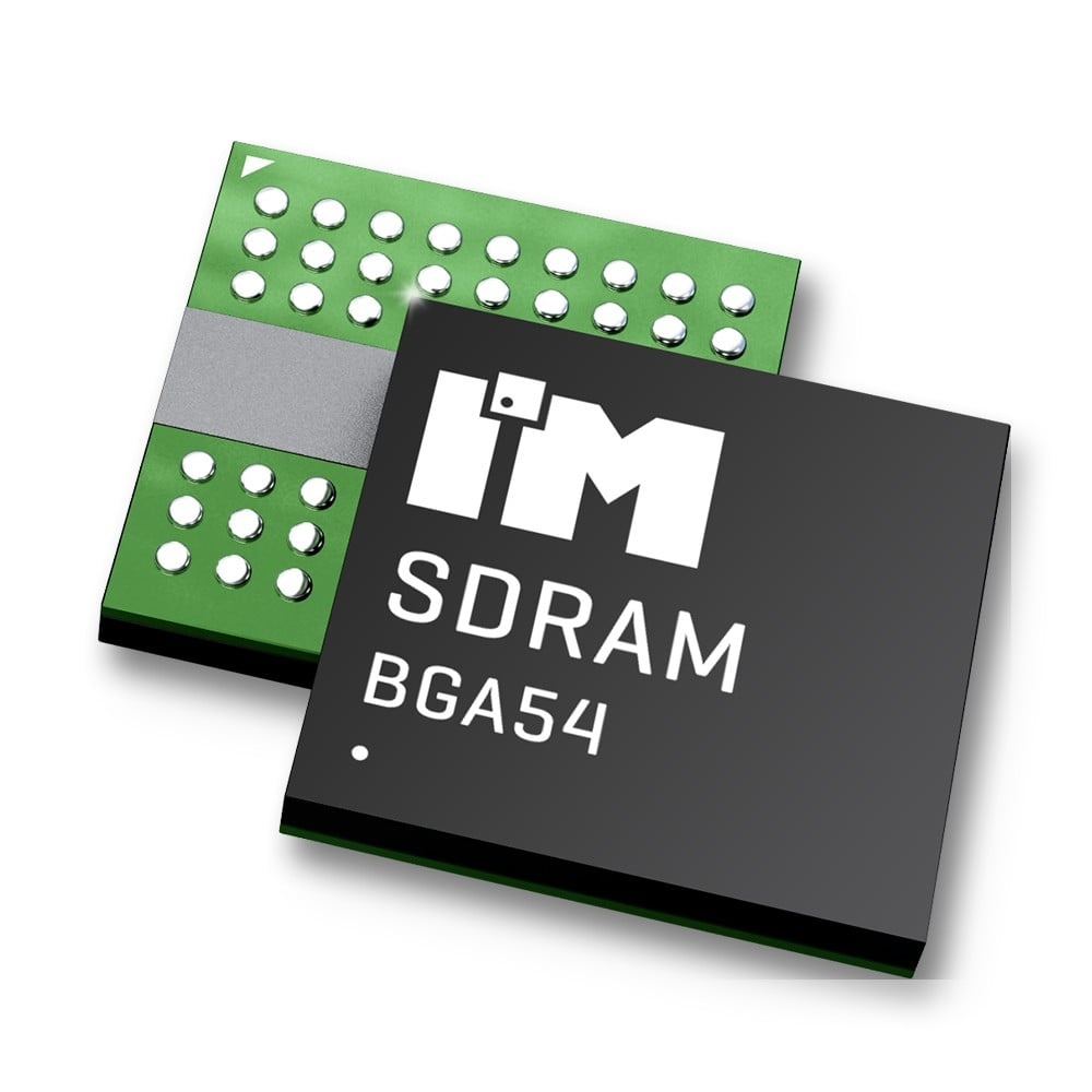
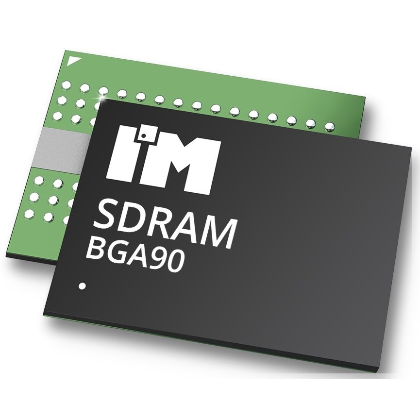
- Package & temperature Supplied in an 84-ball FBGA package (8 mm × 12.5 mm) with specified operating case temperature range of −40°C to 95°C for the industrial option.
Typical Applications
- Industrial systems Industrial equipment requiring DDR2 memory at an extended case temperature range (−40°C to 95°C) can use this device for system memory and buffering.
- Commercial computing platforms Commercial DDR2-based systems that require a 1.8 V SSTL_18 DDR2 interface and programmable latency options for timing tuning.
- Legacy DDR2 designs Systems and modules designed around DDR2-800 (400 MHz) where a 32M × 16, 512 Mbit density device is required.
Unique Advantages
- Industrial temperature support: Specified Tcase range down to −40°C and up to 95°C provides suitability for temperature-challenging environments.
- Flexible timing configuration: Programmable CAS latency (3–7), additive latency settings, and selectable burst lengths allow designers to tune performance to system timing requirements.
- On-die termination and DLL: ODT and on-chip DLL reduce external termination complexity and help align DQ/DQs to CK for reliable high-speed signaling.
- Standard DDR2 signaling: SSTL_18 interface and JEDEC 1.8 V supply range (1.7 V–1.9 V) ensure compatibility with DDR2 system designs that use SSTL_18 signaling levels.
- Compact BGA footprint: 84-ball FBGA package (8 mm × 12.5 mm) offers a compact mounting solution for space-constrained board designs.
- Refresh and low-power modes: Auto Refresh, Self Refresh and Power Down mode support help manage refresh behavior and reduce active power when idle.
Why Choose IM5116D2DDBG-25I?
The IM5116D2DDBG-25I provides a configurable DDR2 SDRAM solution that combines 512 Mbit density in a 32M × 16 organization with DDR2-800 (400 MHz) timing, on-die termination, and programmable latencies. Its 1.8 V supply range and SSTL_18 interface make it suitable for systems built around standard DDR2 signaling, while the industrial temperature option addresses harsher operating environments.
This device is well suited to designers and procurement teams specifying DDR2 memory for existing DDR2 platforms, industrial controllers, or commercial systems that require a compact 84-ball FBGA package and flexible timing options backed by documented device timing and refresh behavior.
To request a quote or submit a purchase inquiry for IM5116D2DDBG-25I, please provide your quantity and delivery requirements and a sales representative will follow up with pricing and availability details.