IM5116SDBBBG-6I
| Part Description |
SDRAM, 512MB, 3.3V, 32MX16, 166M |
|---|---|
| Quantity | 1,912 Available (as of June 15, 2026) |

| Product Category | Memory |
|---|---|
| Manufacturer | Intelligent Memory Ltd. |
| Manufacturing Status | Active |
| Manufacturer Standard Lead Time | 10 Weeks |
| Datasheet |
Specifications & Environmental
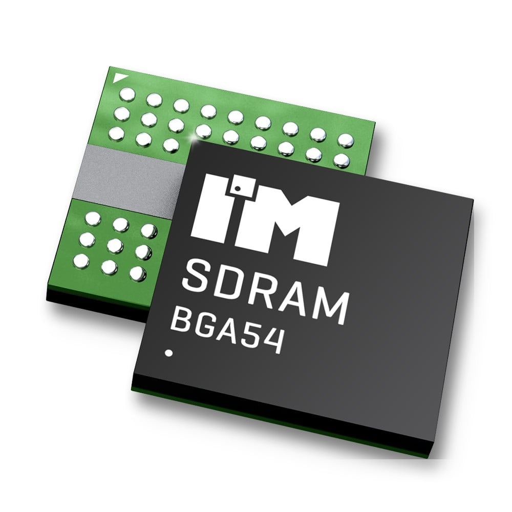
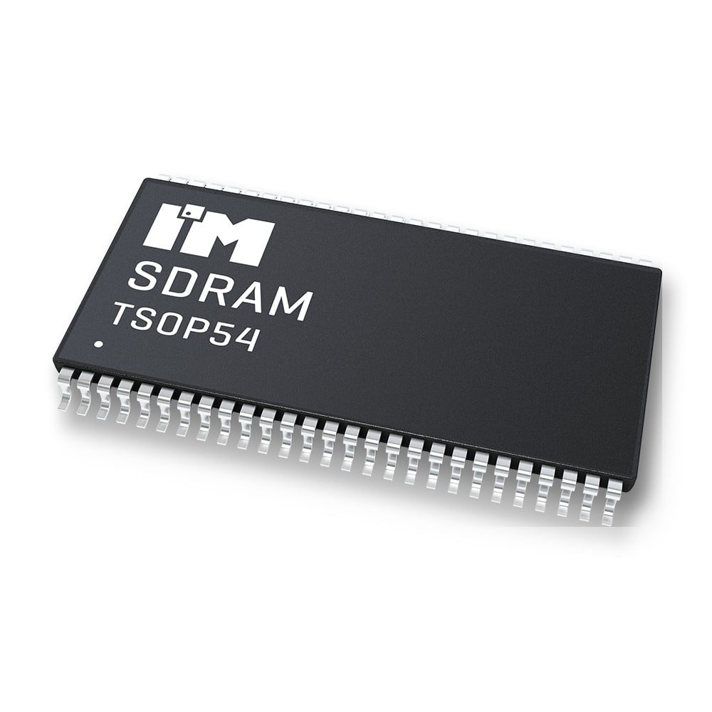
| Device Package | 54-FBGA (8x8) | Memory Format | DRAM | Technology | SDRAM | ||
|---|---|---|---|---|---|---|---|
| Memory Size | 512 Mbit | Access Time | 5.4 ns | Grade | Industrial | ||
| Clock Frequency | 166 MHz | Voltage | 3V ~ 3.6V | Memory Type | Volatile | ||
| Operating Temperature | -40°C ~ 85°C (TA) | Write Cycle Time Word Page | 15 ns | Packaging | 54-TFBGA | ||
| Mounting Method | Volatile | Memory Interface | LVTTL | Memory Organization | 32M x 16 | ||
| Moisture Sensitivity Level | 3 (168 Hours) | RoHS Compliance | ROHS3 Compliant | REACH Compliance | REACH Affected | ||
| Qualification | N/A | ECCN | EAR99 | HTS Code | 8542.32.0028 |
Overview of IM5116SDBBBG-6I – 512MB SDRAM, 3.3V, 32MX16, 166M
The IM5116SDBBBG-6I is a synchronous DRAM device organized as 4 banks × 8Mbit × 16, delivering 512 Mbit of memory capacity on a single 3.3 V device. The part implements full synchronous DRAM architecture with all control, address and data signals referenced to the rising edge of an external clock.
This device is specified for up to 166 MHz system frequency (6 ns clock cycle at CAS latency 3) and supports programmable CAS latencies, multiple burst lengths and refresh modes for use in systems that require externally interfaced SDRAM operating over a -40°C to 85°C ambient range.
Key Features
- Core / Memory Organization Four banks organized as 4 × 8Mbit × 16 (32M ×16) providing a total of 512 Mbit of SDRAM storage.
- Performance System frequency up to 166 MHz (6 ns cycle at CL=3), clock access time tAC = 5.4 ns (CL=3), and access timing options supporting CAS latency 2 and 3.
- Burst and Access Control Programmable burst lengths (1, 2, 4, 8 and full page for sequential; 1, 2, 4, 8 for interleave), programmable wrap sequence (sequential or interleave), and support for multiple burst read with single write operations.
- Refresh and Power Management Auto Refresh and Self Refresh supported with a refresh interval of 8192 cycles/64 ms, plus a Power Down mode for reduced activity.
- Interface LVTTL-compatible interface with single-pulsed RAS, data mask for read/write control, and four-bank control via BA0/BA1 signals.
- Voltage Single 3.3 V ± 0.3 V supply (operating range 3.0 V to 3.6 V).
- Package Available in 54-pin packages including TSOP-II and 54-ball FBGA (8 mm × 8 mm) / 54-TFBGA footprint.
- Operating Temperature Specified for industrial ambient operation from -40°C to 85°C (TA).
Unique Advantages
- High-frequency operation: Up to 166 MHz system frequency (6 ns cycle at CL=3) enables higher sequential and burst throughput where timing margins allow.
- Flexible latency and burst control: Programmable CAS latency (2 or 3) and multiple burst length options allow tuning for system timing and bandwidth needs.
- Four-bank architecture: Interleaved bank operation supports higher random access rates compared to single-bank DRAM by allowing overlapping operations.
- Standard 3.3 V interface: Operates from 3.0 V to 3.6 V with LVTTL signaling for compatibility with common 3.3 V system designs.
- Industrial temperature range: Rated for -40°C to 85°C ambient, supporting deployment in temperature-challenging environments.
- Compact package choices: Offered in 54-pin TSOP-II and 54-ball FBGA (8×8 mm) packages for space-constrained board designs.
Why Choose SDRAM, 512MB, 3.3V, 32MX16, 166M?
The IM5116SDBBBG-6I combines a 4-bank SDRAM architecture with up to 166 MHz operation and programmable latency/burst modes to provide a versatile external memory option for designs requiring synchronous DRAM at 3.3 V. Its support for auto/self refresh, power down, and industry temperature range makes it suitable for systems that need deterministic external memory behavior across varying operating conditions.
This device is suited to engineers and procurement teams looking for a documented, timing-configurable 512 Mbit SDRAM in compact TSOP or FBGA footprints, with clear electrical and timing specifications for system integration.
Request a quote or contact sales to obtain pricing, lead-time and ordering information for the IM5116SDBBBG-6I.