H54G46CYRVX267
| Part Description |
LPDDR4X 2GB (2CH 1CS) 4266Mbps 1.8V/1.1V/0.6V 200-Ball FBGA |
|---|---|
| Quantity | 3,952 Available (as of June 8, 2026) |
| Product Category | Memory |
|---|---|
| Manufacturer | SK Hynix |
| Manufacturing Status | Active |
| Manufacturer Standard Lead Time | Contact Us |
| Datasheet |
Specifications & Environmental
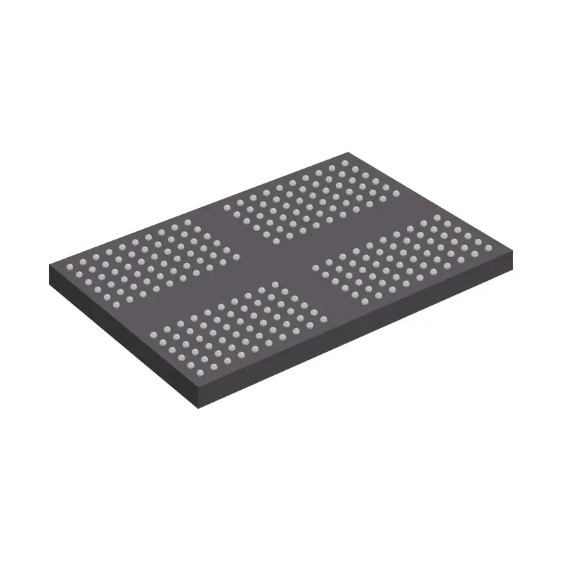
| Device Package | 200-FBGA (10×15) | Memory Format | DRAM | Technology | LPDDR4X | ||
|---|---|---|---|---|---|---|---|
| Memory Size | 2 GB | Access Time | 3.5 ns | Grade | Automotive | ||
| Clock Frequency | 2133 MHz | Voltage | 0.57V ~ 1.95V | Memory Type | Volatile | ||
| Operating Temperature | −40°C – 95°C | Write Cycle Time Word Page | 18 ns | Packaging | 200-FBGA | ||
| Mounting Method | Surface Mount | Memory Interface | Parallel | Memory Organization | 2 × 512M × 16 | ||
| Moisture Sensitivity Level | 3 | RoHS Compliance | Compliant | REACH Compliance | REACH Unknown | ||
| Qualification | AEC-Q100 | ECCN | EAR99 | HTS Code | 8542.32.00.28 |
Overview of H54G46CYRVX267 – 2GB LPDDR4X Automotive DRAM
The H54G46CYRVX267 is an SK hynix 2 GB LPDDR4X automotive memory and mobile DRAM organized as a dual-channel, single-chip-select device (2CH 1CS), each channel on an 8 Gb × 16 die delivering up to 4266 Mbps over a 16-bit data bus. On a 1.8V LPDDR4X triple-rail supply — VDD1 = 1.8V, VDD2 = 1.1V, VDDQ = 0.6V — this low power DRAM suits thermally constrained SoC platforms.
Factory-qualified to AEC-Q100 AIT grade across −40°C to 95°C, this JEDEC-compliant embedded DRAM targets ADAS, in-vehicle infotainment (IVI), digital cockpit, telematics ECU, and industrial embedded designs. RoHS compliant, lead-free, and halogen-free in a 200-ball FBGA (10 mm × 15 mm).
Key Features
- Dual-Channel x16 LPDDR4X Architecture
2 GB as two independent 8 Gb × 16 channels each with 16-bit bus DQ[15:0], differential strobe pairs DQS[1:0]_t/_c, and two DMI pins per channel for write data masking and Data Bus Inversion (DBIdc). - 4266 Mbps Double-Data-Rate Interface
Two data accesses per clock cycle at up to 4266 Mbps (tCK(avg) min = 0.468 ns); single-data-rate command/address over 6-bit CA bus; differential clock CK_t/CK_c and bi-directional differential strobes DQS_t/DQS_c. - Ultra-Low-Voltage Supply — VDDQ = 0.6V
VDD1 = 1.8V (1.70V–1.95V), VDD2 = 1.1V (1.06V–1.17V), VDDQ = 0.6V (0.57V–0.65V); 0.6V VDDQ I/O domain reduces switching power in fanless automotive modules and mobile SoC platforms. - AEC-Q100 AIT Automotive Grade — −40°C to 95°C
Meets AEC-Q100 AIT across −40°C to 95°C; pin-compatible H54G46CYRQX267 extends to −40°C to 105°C (AEC-Q100 AAT) in the same 200-ball FBGA at 4266 Mbps. - Programmable ODT, ZQ Calibration, and Burst Control
Programmable CA ODT and DQ ODT with VSSQ termination (MR11, MR22); DQ ODT RZQ/1–RZQ/6 (240Ω–40Ω) with VOH-compensated output driver; background ZQ calibration; burst length 16 (default), 32, and on-the-fly; programmable RL/WL across FSP[0] and FSP[1]. - Advanced Refresh — Auto TCSR, Per-Bank, and PASR
All-bank and directed per-bank auto refresh; Auto Temperature Compensated Self Refresh (Auto TCSR); Partial Array Self Refresh (PASR) with bank mask (MR16) and segment mask (MR17) to reduce active refresh area and standby power. - 200-Ball FBGA — 10 mm × 15 mm, RoHS, Lead-Free, Halogen-Free
0.80/0.65 mm pitch, 1.00 mm max height; RoHS compliant, lead-free, halogen-free LPDDR4X BGA for space-constrained automotive and embedded board designs.
Typical Applications
- ADAS, Digital Cockpit, and In-Vehicle Infotainment
AEC-Q100 AIT qualification and 4266 Mbps dual-channel bandwidth suit ADAS SoCs, sensor fusion processors, IVI systems, and digital cockpit platforms across the −40°C to 95°C automotive range. - Mobile SoCs and Edge-AI Inference
0.6V VDDQ and dual-channel x16 architecture suit mobile application processors, neural network processors, and edge-AI inference accelerators prioritising bandwidth per milliwatt. - Industrial IoT and Telematics
PASR, Auto TCSR, and −40°C to 95°C operation support industrial IoT gateways, telematics ECUs, and V2X modules needing low power DRAM with adaptive refresh.
Unique Advantages
- AEC-Q100 AIT factory-qualified automotive memory: No additional qualification required, accelerating time-to-market for automotive designs.
- Frequency Set Point (FSP) switching: Dual FSPs enable atomic switch of timing, ODT, and Vref via a single MRW command for zero-gap DVFS in mobile and automotive SoCs.
- On-chip DQS Interval Oscillator: Tracks DQS clock-tree delay drift for adaptive re-training only when needed, reducing system overhead.
- Post Package Repair (PPR): Electrical-fuse-based repair of one failed row per bank per channel enables field yield recovery without package replacement.
Why Choose H54G46CYRVX267?
The H54G46CYRVX267 combines SK hynix LPDDR4X memory with AEC-Q100 AIT qualification, 4266 Mbps dual-channel bandwidth, 0.6V VDDQ low power DRAM architecture, PASR, Auto TCSR, FSP switching, and Post Package Repair in a compact 200-ball FBGA — an automotive memory and embedded DRAM solution for ADAS, digital cockpit, edge-AI, telematics ECU, and industrial IoT platforms.
Request a quote or submit a sales inquiry to receive pricing, availability, and lead-time information for the H54G46CYRVX267.