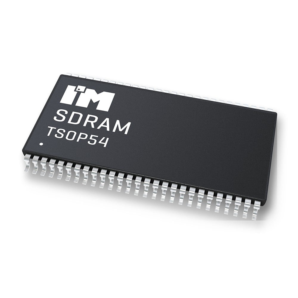
IME5108SDBETG-75I
| Part Description |
ECC SDRAM, 512MB, 3.3V, 64MX8, 1 |
|---|---|
| Quantity | 578 Available (as of June 15, 2026) |

| Product Category | Memory |
|---|---|
| Manufacturer | Intelligent Memory Ltd. |
| Manufacturing Status | Active |
| Manufacturer Standard Lead Time | 12 Weeks |
| Datasheet |
Specifications & Environmental
| Device Package | 54-TSOP II | Memory Format | DRAM | Technology | SDRAM | ||
|---|---|---|---|---|---|---|---|
| Memory Size | 512 Mbit | Access Time | 5.4 ns | Grade | Industrial | ||
| Clock Frequency | 133 MHz | Voltage | 3V ~ 3.6V | Memory Type | Volatile | ||
| Operating Temperature | -40°C ~ 85°C (TA) | Write Cycle Time Word Page | 15 ns | Packaging | 54-TSOP (0.400", 10.16mm Width) | ||
| Mounting Method | Volatile | Memory Interface | LVTTL | Memory Organization | 64M x 8 | ||
| Moisture Sensitivity Level | 3 (168 Hours) | RoHS Compliance | ROHS3 Compliant | REACH Compliance | REACH Affected | ||
| Qualification | N/A | ECCN | EAR99 | HTS Code | 8542.32.0028 |
Overview of IME5108SDBETG-75I – 512 Mbit ECC SDRAM, 64M × 8, 3.3 V, 54‑pin TSOP II
The IME5108SDBETG-75I is a synchronous DRAM device with integrated ECC error correction organized as 4 banks × 16Mbit × 8 (total 512 Mbit). The device implements a full synchronous architecture with all control, address and data signals referenced to the rising edge of an external clock and supports programmable CAS latency and burst operation.
Targeted at systems that require error detection and correction with industrial temperature capability, this device offers 133 MHz system frequency (speed grade -75 at CAS latency 3), a single 3.3 V ±0.3 V supply and a compact 54‑pin TSOP II package for board-level memory subsystems.
Key Features
- Core / Memory Architecture — Four-bank SDRAM organized as 4 × 16Mbit × 8 (64M × 8 total) with integrated ECC error correction for single-device memory protection.
- Performance — Speed grade -75 supports a system frequency of 133 MHz at CAS Latency = 3 and a clock access time (tAC) of 5.4 ns at CL = 3; programmable CAS latency 2 or 3.
- Burst and Access Control — Programmable burst lengths (1, 2, 4, 8, full page for sequential; 1, 2, 4, 8 for interleave), sequential or interleave wrap sequence, and multiple burst read with single write operation.
- Interface — LVTTL input/output interface with single 3.3 V ±0.3 V power supply (operating range 3.0 V to 3.6 V).
- Timing — Clock cycle time tCK = 7.5 ns for CL3 (-75); write cycle time (word/page) 15 ns; random column address every clock (1‑N rule).
- System Reliability — Integrated ECC error correction; auto refresh and self refresh support with 4096 cycles/64 ms refresh interval and single-pulsed RAS interface.
- Power and Modes — Power down mode, automatic and controlled precharge commands to reduce standby power during idle periods.
- Package & Temperature — Available in a 54‑pin TSOP II (0.400" / 10.16 mm width) and specified for industrial operating temperature range −40 °C to +85 °C (Ta).
Typical Applications
- Industrial systems — Memory subsystems in industrial equipment that require extended operating temperature (−40 °C to +85 °C) and error correction.
- Error‑tolerant embedded platforms — Designs that require integrated ECC to improve data integrity within a 3.3 V synchronous DRAM interface.
- Compact board‑level memory modules — Applications needing a 54‑pin TSOP II package for space-constrained PCBs while maintaining synchronous burst and programmable timing features.
Unique Advantages
- Integrated ECC error correction: Built‑in ECC provides on‑chip error detection and correction, improving data integrity without additional external logic.
- Industrial temperature rating: Rated for −40 °C to +85 °C (Ta) to meet extended temperature requirements in harsh environments.
- Flexible timing and burst control: Programmable CAS latency (2, 3), multiple burst lengths and wrap modes allow tuning for system throughput and latency tradeoffs.
- Single 3.3 V supply with LVTTL interface: Simplifies power delivery and signal interfacing in existing 3.3 V system architectures.
- Compact TSOP II package: 54‑pin TSOP II provides a small footprint option for board-level memory integration.
Why Choose IME5108SDBETG-75I?
The IME5108SDBETG-75I combines a four‑bank synchronous DRAM architecture with integrated ECC to deliver a compact, industrial‑rated memory device suitable for systems that need data integrity, programmable timing and burst flexibility. Its 133 MHz speed grade (−75), LVTTL interface and single 3.3 V supply make it straightforward to integrate into established 3.3 V memory subsystems.
This device is well suited to engineers designing industrial or error‑sensitive embedded platforms that require a small‑footprint, ECC‑capable SDRAM with defined timing parameters and refresh behavior. The combination of integrated ECC, industrial temperature range and TSOP II packaging provides a reliable option for long‑term deployments where data integrity and environmental robustness matter.
Request a quote or submit an inquiry to our sales team to discuss pricing, availability and volume options for the IME5108SDBETG-75I.