IS42S16160D-6TL-TR
| Part Description |
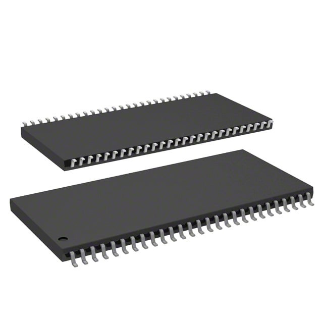
IC DRAM 256MBIT PAR 54TSOP II |
|---|---|
| Quantity | 1,636 Available (as of June 15, 2026) |

| Product Category | Memory |
|---|---|
| Manufacturer | Integrated Silicon Solution Inc |
| Manufacturing Status | Obsolete |
| Manufacturer Standard Lead Time | Contact Us |
| Datasheet |
Specifications & Environmental
| Device Package | 54-TSOP II | Memory Format | DRAM | Technology | SDRAM | ||
|---|---|---|---|---|---|---|---|
| Memory Size | 256 Mbit | Access Time | 5.4 ns | Grade | Commercial | ||
| Clock Frequency | 166 MHz | Voltage | 3V ~ 3.6V | Memory Type | Volatile | ||
| Operating Temperature | 0°C ~ 70°C (TA) | Write Cycle Time Word Page | N/A | Packaging | 54-TSOP (0.400", 10.16mm Width) | ||
| Mounting Method | Volatile | Memory Interface | Parallel | Memory Organization | 16M x 16 | ||
| Moisture Sensitivity Level | 3 (168 Hours) | RoHS Compliance | ROHS3 Compliant | REACH Compliance | REACH Unaffected | ||
| Qualification | N/A | ECCN | EAR99 | HTS Code | 8542.32.0024 |
Overview of IS42S16160D-6TL-TR – IC DRAM 256MBIT PAR 54TSOP II
The IS42S16160D-6TL-TR is a 256‑Mbit synchronous DRAM organized as 16M × 16 with a parallel memory interface in a 54‑pin TSOP‑II package. It uses a pipelined, fully synchronous architecture with all signals referenced to the rising edge of the clock to support high‑speed data transfer in commercial temperature applications.
This device targets designs requiring a compact 256‑Mbit SDRAM solution with programmable burst modes, selectable CAS latency, and standard refresh features for system memory and buffering at clock rates up to 166 MHz.
Key Features
- Memory Organization 16M × 16 configuration delivering 256 Mbit of synchronous DRAM storage in a single device.
- Performance Clock frequency up to 166 MHz (CAS latency = 3) with an access time from clock of 5.4 ns (CAS latency = 3), enabling high‑rate data transfers.
- Synchronous Pipeline Architecture Fully synchronous operation with all inputs/outputs referenced to the positive clock edge and internal bank architecture to hide row access/precharge.
- Programmable Burst and Latency Programmable burst length (1, 2, 4, 8, full page) and burst sequence (sequential/interleave), with CAS latency selectable between 2 and 3 clocks.
- Refresh and Self‑Refresh Auto Refresh (CBR), self‑refresh capability and standard refresh cycles (8K cycles per refresh interval options documented in the datasheet).
- Interface and Logic Levels LVTTL interface for control and address signals and a parallel memory interface for conventional SDRAM system integration.
- Power Single supply operation at 3.3 V ± 0.3 V (3.0 V to 3.6 V specified).
- Package and Temperature 54‑pin TSOP‑II (0.400", 10.16 mm width) with a commercial operating temperature range of 0 °C to +70 °C (TA).
Typical Applications
- Commercial Embedded Systems Use as system memory or external SDRAM for embedded platforms that require 256‑Mbit capacity and synchronous interface timing.
- Data Buffering Employed for high‑throughput buffering in designs that need predictable, clock‑referenced read/write operations and programmable burst behavior.
- Memory Expansion Suitable for adding parallel SDRAM capacity in compact board designs where TSOP‑II packaging and a 3.3 V supply are required.
Unique Advantages
- High clock capability Supports up to 166 MHz operation (CAS = 3), providing fast, clock‑aligned transfers for timing‑sensitive applications.
- Flexible burst and latency control Programmable burst lengths and CAS latency options let designers tune throughput and access timing to system needs.
- Standard power domain Single 3.3 V supply simplifies power rail design and integration with common legacy and commercial systems.
- Compact package 54‑pin TSOP‑II packaging (10.16 mm width) offers a small form factor for space‑constrained boards.
- Built‑in refresh management Auto refresh and self‑refresh modes reduce external refresh handling and help maintain data integrity over standard refresh intervals.
- Synchronous, pipelined operation Predictable, clock‑referenced IO and internal bank architecture optimize throughput and simplify timing analysis.
Why Choose IC DRAM 256MBIT PAR 54TSOP II?
The IS42S16160D-6TL-TR delivers a straightforward 256‑Mbit SDRAM building block with clearly specified timing, programmable burst behavior, and industry‑standard LVTTL signaling. Its 16M × 16 organization, support for up to 166 MHz operation, and 3.3 V single‑supply operation make it suitable for commercial designs that need a compact, synchronous DRAM solution in TSOP‑II packaging.
This device is suited to engineers and procurement teams seeking a documented, timing‑defined SDRAM component for memory expansion, buffering, or system memory duties where commercial temperature operation and standard refresh features meet design requirements.
Request a quote or submit a component inquiry to obtain pricing, availability, and lead‑time information for the IS42S16160D-6TL-TR.