IS42S16160D-6TLI
| Part Description |
IC DRAM 256MBIT PAR 54TSOP II |
|---|---|
| Quantity | 684 Available (as of June 15, 2026) |

| Product Category | Memory |
|---|---|
| Manufacturer | Integrated Silicon Solution Inc |
| Manufacturing Status | Obsolete |
| Manufacturer Standard Lead Time | Contact Us |
| Datasheet |
Specifications & Environmental
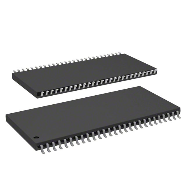
| Device Package | 54-TSOP II | Memory Format | DRAM | Technology | SDRAM | ||
|---|---|---|---|---|---|---|---|
| Memory Size | 256 Mbit | Access Time | 5.4 ns | Grade | Industrial | ||
| Clock Frequency | 166 MHz | Voltage | 3V ~ 3.6V | Memory Type | Volatile | ||
| Operating Temperature | -40°C ~ 85°C (TA) | Write Cycle Time Word Page | N/A | Packaging | 54-TSOP (0.400", 10.16mm Width) | ||
| Mounting Method | Volatile | Memory Interface | Parallel | Memory Organization | 16M x 16 | ||
| Moisture Sensitivity Level | 3 (168 Hours) | RoHS Compliance | ROHS3 Compliant | REACH Compliance | REACH Unaffected | ||
| Qualification | N/A | ECCN | EAR99 | HTS Code | 8542.32.0024 |
Overview of IS42S16160D-6TLI – 256Mbit SDRAM, 54‑TSOP II
The IS42S16160D-6TLI is a 256 Mbit synchronous DRAM organized as 16M × 16 with four internal banks. It implements a pipelined, fully synchronous SDRAM architecture with programmable burst modes and CAS latency options to support high-speed data transfer in memory-buffering applications.
Designed for 3.0 V to 3.6 V systems and offered in a 54‑pin TSOP II package, this device targets designs that require predictable timing, burst read/write capability, and standard SDRAM control using a positive-edge clock reference.
Key Features
- Memory Core 256 Mbit SDRAM organized as 16M × 16 with four internal banks for concurrent row access and hidden precharge.
- Performance Supports up to 166 MHz clock frequency with access time as low as 5.4 ns (CAS latency = 3) and programmable CAS latency of 2 or 3 clocks.
- Burst and Transfer Modes Programmable burst length (1, 2, 4, 8, full page) and selectable sequential or interleave burst sequences; supports burst read/write and burst read/single write operations with burst termination commands.
- Refresh and Low‑Power Options Auto Refresh (CBR) and Self Refresh supported; 8K refresh cycles per specified interval per device grade as indicated in the datasheet.
- Interface and Logic Levels Fully synchronous operation with LVTTL interface and all inputs/outputs referenced to the rising edge of the clock.
- Power Single power supply operation specified across 3.0 V to 3.6 V.
- Package and Temperature Available in a 54‑pin TSOP II (10.16 mm width) package; specified operating ambient temperature range −40°C to +85°C (TA).
Typical Applications
- High‑speed buffering System memory buffering where pipelined synchronous transfers and programmable burst lengths enable sustained data throughput.
- Burst transfer controllers Designs that require deterministic, burst-oriented read/write sequences and selectable CAS latency for timing tuning.
- Embedded memory subsystems Embedded platforms and board‑level designs requiring a 3.0 V–3.6 V SDRAM in a compact 54‑pin TSOP II package.
Unique Advantages
- Flexible timing control: Programmable CAS latency (2 or 3) and selectable burst lengths provide timing flexibility to match system clocking and throughput requirements.
- Pipelined synchronous architecture: Fully synchronous operation with positive-edge clock referencing simplifies timing analysis and integration in synchronous systems.
- Compact board footprint: 54‑pin TSOP II package offers a space-efficient footprint for board designs that require through‑board mounted SDRAM.
- Standard 3.0 V–3.6 V power: Single-supply operation compatible with common 3.3 V system supplies simplifies power rail design.
- Power and data integrity features: Support for Auto Refresh and Self Refresh helps maintain data integrity across refresh cycles and low‑power intervals.
Why Choose IS42S16160D-6TLI?
The IS42S16160D-6TLI combines a 16M × 16 organization and four-bank pipelined SDRAM architecture to deliver predictable, high-speed synchronous memory behavior for designs that depend on burst transfers and low access latency. Its programmable timing options and standard LVTTL interface make it suitable for systems requiring deterministic memory timing and flexible throughput tuning.
This device is appropriate for engineers specifying compact, board‑level SDRAM in systems running from a 3.0 V–3.6 V supply and operating over an extended ambient temperature range to −40°C to +85°C. The combination of burst modes, refresh features, and compact 54‑pin TSOP II packaging provides a practical balance of performance and board real estate for embedded memory subsystems.
If you need pricing, availability, or a formal quote for IS42S16160D-6TLI, request a quote or submit a product inquiry and our team will respond with the requested information.