IS42S16160D-75ETLI
| Part Description |
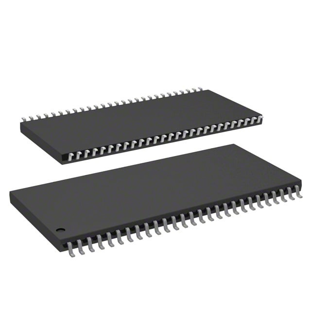
IC DRAM 256MBIT PAR 54TSOP II |
|---|---|
| Quantity | 956 Available (as of June 15, 2026) |
| Product Category | Memory |
|---|---|
| Manufacturer | Integrated Silicon Solution Inc |
| Manufacturing Status | Obsolete |
| Manufacturer Standard Lead Time | Contact Us |
| Datasheet |
Specifications & Environmental
| Device Package | 54-TSOP II | Memory Format | DRAM | Technology | SDRAM | ||
|---|---|---|---|---|---|---|---|
| Memory Size | 256 Mbit | Access Time | 5.5 ns | Grade | Industrial | ||
| Clock Frequency | 133 MHz | Voltage | 3V ~ 3.6V | Memory Type | Volatile | ||
| Operating Temperature | -40°C ~ 85°C (TA) | Write Cycle Time Word Page | N/A | Packaging | 54-TSOP (0.400", 10.16mm Width) | ||
| Mounting Method | Volatile | Memory Interface | Parallel | Memory Organization | 16M x 16 | ||
| Moisture Sensitivity Level | 3 (168 Hours) | RoHS Compliance | ROHS3 Compliant | REACH Compliance | REACH Unaffected | ||
| Qualification | N/A | ECCN | EAR99 | HTS Code | 8542.32.0024 |
Overview of IS42S16160D-75ETLI – IC DRAM 256MBIT PAR 54TSOP II
The IS42S16160D-75ETLI is a 256 Mbit synchronous DRAM organized as 16M × 16 with a parallel memory interface and 54‑pin TSOP II packaging. The device uses a pipeline architecture with fully synchronous operation where all signals reference the rising edge of the clock.
This SDRAM targets designs that require a 256 Mbit parallel memory component with programmable burst operation, selectable CAS latency, and built‑in refresh capabilities for maintained data integrity across operating conditions.
Key Features
- Memory Core and Organization The device is a 256 Mbit SDRAM organized as 16M × 16 with internal bank architecture to hide row access and precharge latency.
- Performance Clock frequency rating up to 133 MHz with an access time of 5.5 ns (specified for the -75 timing grade).
- Programmable Timing and Burst Programmable burst length (1, 2, 4, 8, full page) and burst sequence (sequential/interleave); selectable CAS latency options (2 or 3 clocks).
- Refresh and Self‑Refresh Supports auto refresh (CBR) and self refresh with 8K refresh cycles; refresh intervals vary by device grade as specified in the datasheet.
- Interface and I/O LVTTL-compatible interface with parallel data bus and random column address capability every clock cycle.
- Power Single power supply operation across 3.0 V to 3.6 V.
- Package 54‑pin TSOP II package (0.400", 10.16 mm width) for surface mounting.
- Operating Temperature Specified operating range of -40 °C to +85 °C (TA) for industrial applications.
Typical Applications
- Parallel memory subsystems Designed for systems requiring a 16‑bit parallel SDRAM interface and 256 Mbit memory density.
- High‑throughput buffering Suited to designs that use programmable burst transfers and random column access for frequent sequential data operations.
- Embedded and industrial electronics Intended for designs that need industrial temperature range operation and standard 3.3 V single‑supply DRAM.
Unique Advantages
- Flexible timing options: Programmable CAS latency (2, 3) and multiple burst lengths enable tuning for system timing and throughput requirements.
- Built‑in refresh management: Auto and self refresh modes with 8K refresh cycles reduce external refresh controller complexity.
- Wide supply tolerance: Operates across 3.0 V to 3.6 V single supply for compatibility with standard 3.3 V systems.
- Compact surface‑mount package: 54‑pin TSOP II (10.16 mm width) provides a space-efficient footprint for high‑density board designs.
- Industrial temperature rating: Specified operation from -40 °C to +85 °C supports designs requiring extended ambient ranges.
- Deterministic synchronous operation: Fully synchronous design with LVTTL interface and pipeline architecture aligns signals to the rising clock edge for predictable timing.
Why Choose IC DRAM 256MBIT PAR 54TSOP II?
The IS42S16160D-75ETLI provides a verified 256 Mbit synchronous DRAM solution tailored for parallel bus systems that need programmable burst behavior, selectable CAS latency, and robust refresh management. Its 16M × 16 organization, 133 MHz clock rating (5.5 ns access time), and single 3.0–3.6 V supply make it suitable for designs demanding predictable synchronous memory performance in a compact TSOP II package.
This device is appropriate for engineers designing embedded or industrial systems that require straightforward integration of a parallel SDRAM component with industrial temperature support and standard LVTTL signaling. The combination of programmable timing, internal bank architecture, and refresh capabilities helps simplify memory subsystem design while maintaining required throughput and data retention behaviors.
Request a quote or submit an inquiry to obtain pricing and availability for the IS42S16160D-75ETLI.