IS42S16160D-7BLI-TR
| Part Description |
IC DRAM 256MBIT PAR 54TFBGA |
|---|---|
| Quantity | 1,131 Available (as of June 14, 2026) |

| Product Category | Memory |
|---|---|
| Manufacturer | Integrated Silicon Solution Inc |
| Manufacturing Status | Obsolete |
| Manufacturer Standard Lead Time | Contact Us |
| Datasheet |
Specifications & Environmental
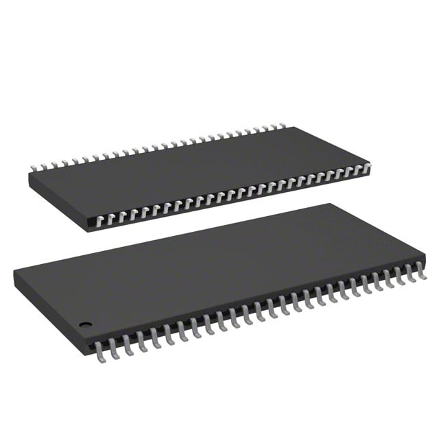
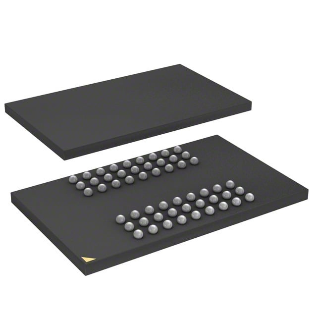
| Device Package | 54-TW-BGA (8x13) | Memory Format | DRAM | Technology | SDRAM | ||
|---|---|---|---|---|---|---|---|
| Memory Size | 256 Mbit | Access Time | 5.4 ns | Grade | Industrial | ||
| Clock Frequency | 143 MHz | Voltage | 3V ~ 3.6V | Memory Type | Volatile | ||
| Operating Temperature | -40°C ~ 85°C (TA) | Write Cycle Time Word Page | N/A | Packaging | 54-TFBGA | ||
| Mounting Method | Volatile | Memory Interface | Parallel | Memory Organization | 16M x 16 | ||
| Moisture Sensitivity Level | 3 (168 Hours) | RoHS Compliance | ROHS3 Compliant | REACH Compliance | REACH Unaffected | ||
| Qualification | N/A | ECCN | EAR99 | HTS Code | 8542.32.0024 |
Overview of IS42S16160D-7BLI-TR – IC DRAM 256MBIT PAR 54TFBGA
The IS42S16160D-7BLI-TR is a 256‑Mbit synchronous DRAM organized as 16M × 16, manufactured by ISSI (Integrated Silicon Solution Inc). It implements a pipelined, fully synchronous architecture with internal bank management to accelerate row access and precharge.
Designed for systems that require parallel, high‑speed volatile memory, this device delivers programmable burst modes, selectable CAS latency, and refresh control for applications demanding predictable, clock‑referenced memory behavior. It operates from a 3.0 V to 3.6 V supply and is available in a 54‑ball TFBGA package.
Key Features
- Memory Core — 256 Mbit SDRAM organized as 16M × 16 with internal bank architecture (4 banks) for hidden row access and precharge.
- Performance & Timing — Clock frequency options include 166 MHz and 143 MHz; the -7 timing option specifies 143 MHz with an access time from clock of 5.4 ns (CAS latency = 3).
- Programmable Burst & CAS — Programmable burst lengths (1, 2, 4, 8, full page) and burst sequence (sequential/interleave); programmable CAS latency of 2 or 3 clocks.
- Refresh & Low‑Power Modes — Supports Auto Refresh (CBR) and Self Refresh with 8K refresh cycles selectable for 16 ms or 64 ms intervals depending on grade.
- Interface — LVTTL compatible signals with fully synchronous operation; random column access every clock cycle and burst read/write capability.
- Power — Single power supply: 3.3 V ± 0.3 V (specified supply range 3.0 V to 3.6 V).
- Package — 54‑TFBGA (54‑ball BGA, 8 × 13) surface‑mount package for compact board integration.
- Operating Temperature — Industrial range: −40 °C to +85 °C (TA) as specified for this device.
Typical Applications
- High‑speed memory buffering — Use as parallel SDRAM buffer memory in systems that require predictable, clocked data transfer at up to the device’s rated clock frequency.
- Embedded system memory — Suitable for designs that need 256 Mbit of volatile synchronous DRAM in a compact BGA package.
- System board integration — Fits applications requiring a 54‑ball TFBGA footprint and a single 3.3 V supply with industrial temperature operation.
Unique Advantages
- Deterministic synchronous operation — Fully synchronous design with all signals referenced to the rising clock edge simplifies timing analysis and system integration.
- Flexible data transfer modes — Programmable burst lengths and sequence plus burst termination options enable optimized throughput for different access patterns.
- Selectable latency and timing — CAS latency options (2, 3 clocks) and multiple timing grades allow tradeoffs between speed and system timing constraints.
- Robust refresh options — Auto and self‑refresh modes with selectable 8K refresh intervals (16 ms or 64 ms) support a range of power and data‑retention scenarios.
- Compact BGA package — 54‑ball TFBGA (8 × 13) provides a small board footprint for space‑constrained designs.
- Industrial temperature support — Specified operation from −40 °C to +85 °C for deployment in temperature‑challenging environments.
Why Choose IS42S16160D-7BLI-TR?
The IS42S16160D-7BLI-TR positions itself as a practical, clocked 256‑Mbit SDRAM solution for designs that require synchronous, parallel memory with programmable burst behavior and selectable CAS latency. Its combination of 16M × 16 organization, internal bank management, and LVTTL interface delivers predictable timing and throughput for system designers.
With a single 3.3 V supply range, industrial temperature rating, and a compact 54‑TFBGA package, this device is suited to embedded and board‑level memory implementations where predictable synchronous performance and a small footprint are important. Manufactured by ISSI, the part carries the documented timing, refresh and interface capabilities engineers rely on when specifying SDRAM.
If you need pricing, availability, or a formal quote for the IS42S16160D-7BLI-TR, submit a request for quote or contact sales to obtain product pricing and lead‑time information.