IS42S16160D-7TLI
| Part Description |
IC DRAM 256MBIT PAR 54TSOP II |
|---|---|
| Quantity | 571 Available (as of June 15, 2026) |

| Product Category | Memory |
|---|---|
| Manufacturer | Integrated Silicon Solution Inc |
| Manufacturing Status | Obsolete |
| Manufacturer Standard Lead Time | Contact Us |
| Datasheet |
Specifications & Environmental
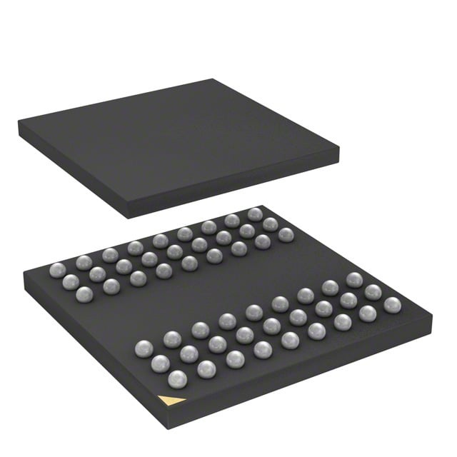
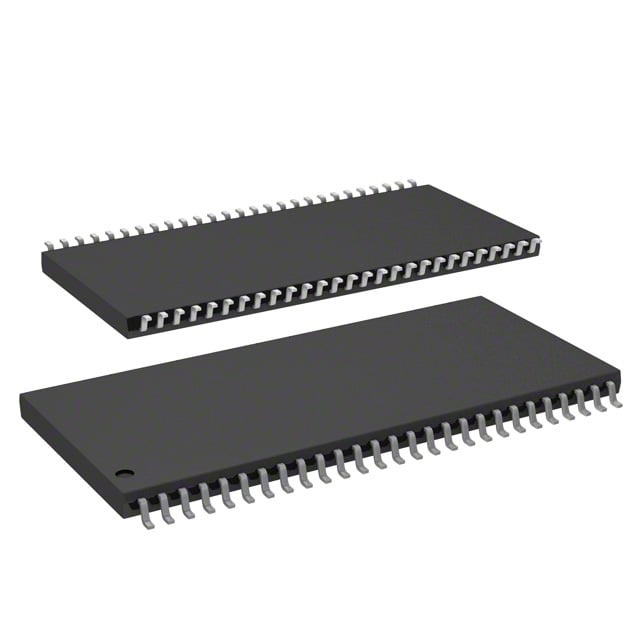
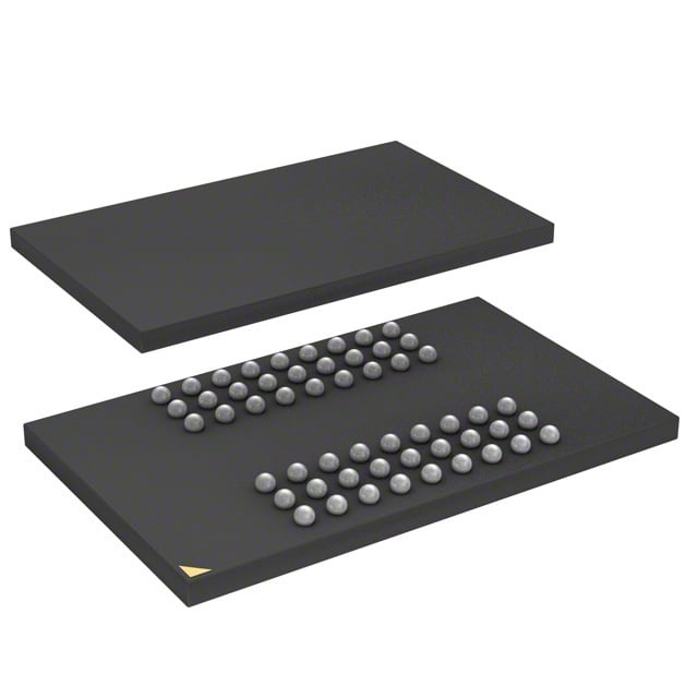
| Device Package | 54-TSOP II | Memory Format | DRAM | Technology | SDRAM | ||
|---|---|---|---|---|---|---|---|
| Memory Size | 256 Mbit | Access Time | 5.4 ns | Grade | Industrial | ||
| Clock Frequency | 143 MHz | Voltage | 3V ~ 3.6V | Memory Type | Volatile | ||
| Operating Temperature | -40°C ~ 85°C (TA) | Write Cycle Time Word Page | N/A | Packaging | 54-TSOP (0.400", 10.16mm Width) | ||
| Mounting Method | Volatile | Memory Interface | Parallel | Memory Organization | 16M x 16 | ||
| Moisture Sensitivity Level | 3 (168 Hours) | RoHS Compliance | ROHS3 Compliant | REACH Compliance | REACH Unaffected | ||
| Qualification | N/A | ECCN | EAR99 | HTS Code | 8542.32.0024 |
Overview of IS42S16160D-7TLI – IC DRAM 256MBIT PAR 54TSOP II
The IS42S16160D-7TLI is a 256‑Mbit synchronous DRAM organized as 16M × 16 with a parallel memory interface. The device implements a pipeline architecture and fully synchronous operation with all signals referenced to the rising edge of the clock to support high‑speed data transfer.
Designed for systems that require high‑frequency, programmable burst memory, the device delivers selectable CAS latency and burst modes, integrated bank management for row access/precharge, and operation from a single 3.3V supply (3.0–3.6V) across a wide temperature range.
Key Features
- Core / Architecture Pipeline architecture with fully synchronous operation; all I/O referenced to the positive clock edge for predictable timing.
- Memory Organization 256 Mbit density organized as 16M × 16 with internal bank architecture (4 banks) to hide row access and precharge cycles.
- Performance Supports a clock frequency up to 143 MHz (‑7 speed grade) and an access time from clock of 5.4 ns (CAS latency = 3).
- Programmable Burst and Latency Programmable burst lengths (1, 2, 4, 8, full page) and burst sequence (sequential/interleave); selectable CAS latency of 2 or 3 clocks.
- Refresh and Self‑Maintenance Auto Refresh (CBR) and Self Refresh supported with 8K refresh cycles; refresh interval options include 16 ms (A2 grade) or 64 ms (commercial/industrial/A1 grade) as specified.
- Interface and Signaling LVTTL interface with parallel memory bus for burst read/write and burst read/single write operations; random column address every clock cycle.
- Power Single power supply: 3.3 V ±0.3 V (3.0–3.6 V operational range).
- Package & Temperature Available in a 54‑pin TSOP‑II (54‑TSOP, 10.16 mm width) package; operating temperature range listed at −40°C to +85°C (TA).
Typical Applications
- High‑speed data buffering Use where pipeline, synchronous DRAM is required to support continuous, clock‑referenced data transfers.
- Burst‑mode memory subsystems Suitable for designs that leverage programmable burst lengths and burst sequencing for block transfers.
- Embedded system memory expansion Provides parallel SDRAM capacity in systems needing 256‑Mbit modules with selectable CAS latency and refresh options.
Unique Advantages
- High‑frequency operation: The ‑7 speed grade supports up to 143 MHz clocking with 5.4 ns access time (CL=3), enabling faster synchronous transfers.
- Flexible burst control: Programmable burst lengths and sequence (sequential/interleave) let designers match memory behavior to system transfer patterns.
- Banked architecture: Internal 4‑bank organization hides row access/precharge latency, improving effective throughput for interleaved access.
- Wide operating voltage window: Single 3.3 V supply with specified 3.0–3.6 V range simplifies power supply design while meeting SDRAM requirements.
- Industrial temperature rating: Specified operation from −40°C to +85°C (TA) supports deployments in thermally demanding environments.
- Standard TSOP‑II package: Compact 54‑TSOP II package (10.16 mm width) provides a standardized footprint for board‑level integration.
Why Choose IC DRAM 256MBIT PAR 54TSOP II?
The IS42S16160D-7TLI offers a combination of synchronous pipeline architecture, banked memory organization, and programmable burst and latency controls to deliver consistent, clock‑referenced performance for parallel SDRAM applications. Its 16M × 16 organization and 256‑Mbit density make it suitable for systems that require medium‑density SDRAM with predictable timing characteristics.
This device is well suited for designers who need a standard TSOP‑II packaged SDRAM with industrial temperature range support and configurable timing/refresh behaviors. The documented timing, refresh options, and single‑supply operation provide a clear basis for system integration and long‑term deployment planning.
Request a quote or submit an inquiry for pricing and availability to obtain lead‑time and volume pricing details for the IS42S16160D-7TLI.