IS42S16160G-5BL
| Part Description |
IC DRAM 256MBIT PAR 54TFBGA |
|---|---|
| Quantity | 209 Available (as of June 15, 2026) |

| Product Category | Memory |
|---|---|
| Manufacturer | Integrated Silicon Solution Inc |
| Manufacturing Status | Obsolete |
| Manufacturer Standard Lead Time | Contact Us |
| Datasheet |
Specifications & Environmental
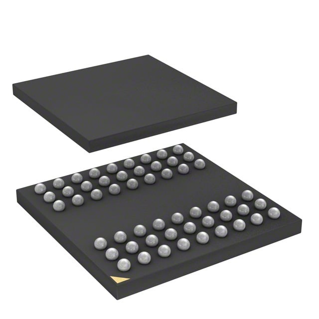
| Device Package | 54-TFBGA (8x8) | Memory Format | DRAM | Technology | SDRAM | ||
|---|---|---|---|---|---|---|---|
| Memory Size | 256 Mbit | Access Time | 5 ns | Grade | Commercial | ||
| Clock Frequency | 200 MHz | Voltage | 3V ~ 3.6V | Memory Type | Volatile | ||
| Operating Temperature | 0°C ~ 70°C (TA) | Write Cycle Time Word Page | N/A | Packaging | 54-TFBGA | ||
| Mounting Method | Volatile | Memory Interface | Parallel | Memory Organization | 16M x 16 | ||
| Moisture Sensitivity Level | 3 (168 Hours) | RoHS Compliance | ROHS3 Compliant | REACH Compliance | REACH Unaffected | ||
| Qualification | N/A | ECCN | EAR99 | HTS Code | 8542.32.0024 |
Overview of IS42S16160G-5BL – IC DRAM 256MBIT PAR 54TFBGA
The IS42S16160G-5BL is a 256 Mbit synchronous DRAM (SDRAM) organized as 16M × 16 with internal banks and a parallel memory interface. It uses a pipelined architecture and fully synchronous timing referenced to the rising edge of the clock to support high-speed data transfer.
Targeted for systems that require a parallel SDRAM solution in a compact 54-ball TFBGA package, the device provides programmable burst control, selectable CAS latency, and standard refresh/self-refresh capabilities while operating from a single 3.0 V–3.6 V supply (3.3 V ±0.3 V per datasheet).
Key Features
- Memory Core 256 Mbit SDRAM organized as 16M × 16 (4M × 16 × 4 banks) for parallel data storage and banked access.
- Clock and Timing Supports clock frequencies up to 200 MHz with programmable CAS latency (2 or 3 clocks) and an access time from clock as low as 5 ns (per datasheet timing table).
- Burst and Sequencing Programmable burst lengths (1, 2, 4, 8, full page) and selectable burst sequence (sequential or interleave) for flexible data transfer patterns.
- Refresh and Retention Auto refresh and self-refresh supported; 8K refresh cycles with options of 32 ms (A2 grade) or 64 ms (commercial/A1 grade) as specified in the datasheet.
- Interface LVTTL-compatible interface signals with fully synchronous operation referencing a positive clock edge.
- Power Single power supply operation; specified voltage range 3.0 V–3.6 V (datasheet: 3.3 V ±0.3 V).
- Package and Temperature 54-ball TFBGA (8 × 8) package; commercial operating temperature range 0°C to +70°C (TA).
Typical Applications
- High-speed buffer memory Use where parallel SDRAM buffering and burst transfers are required to support sustained data throughput.
- Embedded system memory Suitable for designs that need a compact 54-ball BGA SDRAM device with banked access and programmable burst control.
- Legacy parallel SDRAM interfaces Integrates with systems using a parallel SDRAM interface and LVTTL-compatible signaling.
Unique Advantages
- Banked, pipelined architecture Internal bank structure hides row access/precharge and supports pipeline operation for efficient high-speed transfers.
- Flexible burst control Programmable burst lengths and sequences enable optimized data block transfers for a range of access patterns.
- Selectable CAS latency CAS latency options (2 or 3 clocks) allow designers to trade timing for frequency per system requirements.
- Standard refresh modes Auto and self-refresh with 8K refresh cycles (32 ms or 64 ms options) provide standard DRAM retention management.
- Compact BGA footprint 54-ball TFBGA (8×8) package reduces PCB area while providing the necessary ballout for parallel SDRAM connectivity.
Why Choose IS42S16160G-5BL?
The IS42S16160G-5BL positions itself as a compact, banked 256 Mbit SDRAM solution for designs requiring a parallel memory interface and programmable burst behavior. Its support for up to 200 MHz clocking, selectable CAS latency, and standard refresh/self-refresh modes make it suited to systems that need predictable synchronous DRAM performance within a 54-ball TFBGA footprint.
This device is appropriate for engineers specifying parallel SDRAM for embedded or legacy systems where a single 3.0 V–3.6 V supply, commercial temperature range (0°C to +70°C), and LVTTL signaling align with system design constraints. The IS42S16160G-5BL’s feature set delivers scalable memory capacity and timing flexibility while maintaining a small board-level footprint.
Request a quote or submit a pricing inquiry to receive availability and lead-time information for the IS42S16160G-5BL.