IS42S16160G-6BL
| Part Description |
IC DRAM 256MBIT PAR 54TFBGA |
|---|---|
| Quantity | 804 Available (as of June 15, 2026) |

| Product Category | Memory |
|---|---|
| Manufacturer | Integrated Silicon Solution Inc |
| Manufacturing Status | Obsolete |
| Manufacturer Standard Lead Time | Contact Us |
| Datasheet |
Specifications & Environmental
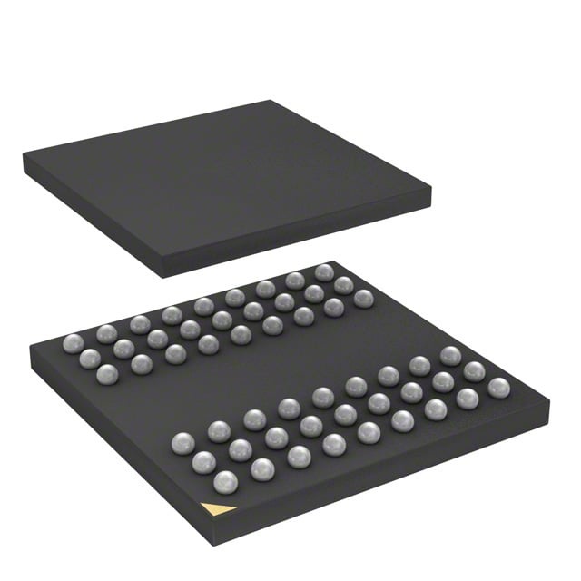
| Device Package | 54-TFBGA (8x8) | Memory Format | DRAM | Technology | SDRAM | ||
|---|---|---|---|---|---|---|---|
| Memory Size | 256 Mbit | Access Time | 5.4 ns | Grade | Commercial | ||
| Clock Frequency | 166 MHz | Voltage | 3V ~ 3.6V | Memory Type | Volatile | ||
| Operating Temperature | 0°C ~ 70°C (TA) | Write Cycle Time Word Page | N/A | Packaging | 54-TFBGA | ||
| Mounting Method | Volatile | Memory Interface | Parallel | Memory Organization | 16M x 16 | ||
| Moisture Sensitivity Level | 3 (168 Hours) | RoHS Compliance | ROHS3 Compliant | REACH Compliance | REACH Unaffected | ||
| Qualification | N/A | ECCN | EAR99 | HTS Code | 8542.32.0024 |
Overview of IS42S16160G-6BL – IC DRAM 256MBIT PAR 54TFBGA
The IS42S16160G-6BL is a 256 Mbit synchronous DRAM (SDRAM) organized as 16M × 16 with a parallel memory interface in a 54-ball TFBGA (8×8) package. It uses a pipelined, fully synchronous architecture with signals referenced to the rising edge of the clock to support high-speed data transfer in commercial-temperature systems.
Designed for applications requiring a compact, 3.3 V single-supply SDRAM device, this part provides programmable burst and latency options plus refresh and self-refresh capabilities to support common system memory buffering and high-throughput data paths.
Key Features
- Memory Core 256 Mbit SDRAM organized as 16M × 16 with internal bank architecture for row access and precharge management.
- Synchronous Operation & Timing Fully synchronous operation with all I/O referenced to the positive clock edge; typical clock frequency supported at 166 MHz and access time of 5.4 ns (–6 speed grade).
- Programmable Burst & CAS Programmable burst lengths (1, 2, 4, 8, full page) and programmable burst sequence (sequential/interleave). CAS latency selectable (2 or 3 clocks).
- Refresh & Power Management Auto-refresh and self-refresh support with standard 8K refresh cycles (commercial: 8K/64 ms) to maintain data integrity.
- Interface & Signaling Parallel memory interface with LVTTL signaling for control and data paths.
- Power Single power supply: nominal 3.3 V (range 3.0 V to 3.6 V).
- Package & Temperature 54-ball TFBGA (8×8) package; specified operating temperature range 0°C to 70°C (TA) for the commercial variant.
Typical Applications
- Embedded systems requiring synchronous DRAM Use as a 256 Mbit parallel SDRAM device for system memory and buffering where a compact 54-ball BGA package is required.
- High-speed data buffering Pipeline architecture and 166 MHz clock support high-throughput read/write bursts for transient data storage and buffering tasks.
- Board-level memory expansion 16M × 16 organization and programmable burst modes enable flexible integration as a parallel DRAM resource on complex PCBs.
Unique Advantages
- Compact BGA footprint: The 54-ball TFBGA (8×8) package reduces board area compared with larger DIP/TSOP options while retaining full SDRAM capability.
- Flexible performance scaling: Programmable CAS latency and burst length/sequence let designers tune throughput and latency to match system timing requirements.
- Synchronous pipeline architecture: All signals referenced to the positive clock edge and internal bank management help support continuous high-speed transfers.
- Standard single-supply operation: 3.3 V nominal supply (3.0–3.6 V) simplifies power-rail design in systems already using 3.3 V logic.
- Refresh and low-power readiness: Auto-refresh and self-refresh modes with 8K refresh cycles preserve data with minimal host intervention.
- Deterministic timing: Documented access times (5.4 ns at the –6 speed grade) and clock-frequency support provide predictable memory performance.
Why Choose IS42S16160G-6BL?
The IS42S16160G-6BL positions itself as a compact, commercially rated 256 Mbit SDRAM solution for designs that need synchronous, parallel DRAM with programmable timing and burst features. Its 16M × 16 organization, LVTTL interface, and support for auto/self-refresh offer a balance of performance and system-level flexibility.
This device is suited to designers and procurement teams specifying board-level SDRAM for embedded systems, high-speed buffering, and memory expansion where a 54-ball TFBGA package and 0°C to 70°C operating range match system requirements. The combination of programmable latency, burst modes, and documented timing simplifies integration and validation in deterministic memory subsystems.
Request a quote or submit an inquiry for pricing and availability for the IS42S16160G-6BL to evaluate lead times and ordering options.