IS42S16160G-6TL-TR
| Part Description |
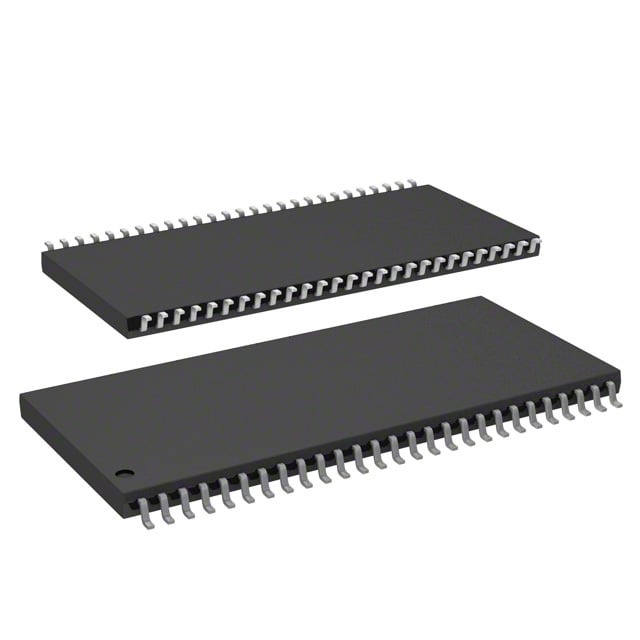
IC DRAM 256MBIT PAR 54TSOP II |
|---|---|
| Quantity | 767 Available (as of June 15, 2026) |

| Product Category | Memory |
|---|---|
| Manufacturer | Integrated Silicon Solution Inc |
| Manufacturing Status | Obsolete |
| Manufacturer Standard Lead Time | Contact Us |
| Datasheet |
Specifications & Environmental
| Device Package | 54-TSOP II | Memory Format | DRAM | Technology | SDRAM | ||
|---|---|---|---|---|---|---|---|
| Memory Size | 256 Mbit | Access Time | 5.4 ns | Grade | Commercial | ||
| Clock Frequency | 166 MHz | Voltage | 3V ~ 3.6V | Memory Type | Volatile | ||
| Operating Temperature | 0°C ~ 70°C (TA) | Write Cycle Time Word Page | N/A | Packaging | 54-TSOP (0.400", 10.16mm Width) | ||
| Mounting Method | Volatile | Memory Interface | Parallel | Memory Organization | 16M x 16 | ||
| Moisture Sensitivity Level | 3 (168 Hours) | RoHS Compliance | ROHS3 Compliant | REACH Compliance | REACH Unaffected | ||
| Qualification | N/A | ECCN | EAR99 | HTS Code | 8542.32.0024 |
Overview of IS42S16160G-6TL-TR – IC DRAM 256MBIT PAR 54TSOP II
The IS42S16160G-6TL-TR is a 256Mbit synchronous DRAM (SDRAM) organized as 16M × 16 with a parallel memory interface. It implements a fully synchronous pipeline architecture with internal bank management to support high-speed data transfer for board-level memory subsystems.
Designed for commercial-temperature applications, the device operates from a 3.3V ±0.3V supply and is supplied in a 54-pin TSOP-II package. Typical use cases include systems requiring a compact 256Mbit SDRAM footprint with programmable burst and latency options.
Key Features
- Memory Architecture 256Mbit SDRAM organized as 16M × 16 with internal bank architecture (4 banks) to improve access efficiency and hide row access/precharge latency.
- Performance Supports clock frequencies including 166 MHz (part -6 timing), with CAS latency options (2 or 3 clocks) and an access time from clock of approximately 5.4 ns.
- Programmable Burst and Latency Programmable burst lengths (1, 2, 4, 8, full page) and selectable burst sequences (sequential or interleave) for flexible memory transfer patterns.
- Refresh and Power Management Supports Auto Refresh and Self Refresh. Refresh cycle counts include 8K/64ms for commercial/industrial operation and 8K/32ms for the A2 option.
- Interface and Signaling Fully synchronous operation with LVTTL-compatible interface; all signals referenced to the rising edge of the clock for deterministic timing.
- Single-Supply Operation Single 3.3V ±0.3V power supply simplifies system power design.
- Package and Temperature Available in a 54-pin TSOP-II (0.400", 10.16mm width) package and specified for commercial temperature range 0°C to +70°C.
Typical Applications
- Board-level Memory Subsystems Use as a compact 256Mbit SDRAM option where a 54-pin TSOP-II footprint and parallel SDRAM interface are required.
- Embedded Systems (Commercial Temperature) Suitable for designs operating within 0°C to +70°C that need synchronous DRAM with programmable burst and latency control.
- Memory Expansion on Consumer and Industrial PCBs Provides parallel SDRAM capacity and timing flexibility for systems requiring deterministic, clock-referenced memory access.
Unique Advantages
- Synchronous SDRAM with Banked Architecture: Internal bank structure and fully synchronous operation enable pipelined access and improved throughput for sequential and random accesses.
- Configurable Performance: Multiple clock-frequency options and selectable CAS latency (2 or 3) plus programmable burst lengths let designers balance latency and throughput.
- Standard TSOP-II Footprint: 54-pin TSOP-II package simplifies board integration where space and standard package form-factor are constraints.
- Single 3.3V Supply: Operates from a single 3.3V ±0.3V supply to align with common system rails and simplify power distribution.
- Flexible Refresh Modes: Supports Auto Refresh and Self Refresh with defined refresh counts (8K/64ms commercial/industrial; 8K/32ms for A2 option) to meet system retention requirements.
- LVTTL-Compatible Interface: Clock-referenced LVTTL signaling ensures predictable timing for synchronous system designs.
Why Choose IS42S16160G-6TL-TR?
The IS42S16160G-6TL-TR provides a compact, programmable 256Mbit SDRAM solution targeted at designs that require a clocked, parallel memory interface in a 54-pin TSOP-II package. Its combination of banked architecture, selectable CAS latency, programmable burst modes, and single-supply 3.3V operation makes it suitable for commercial-temperature systems that need deterministic, high-speed memory behavior.
Backed by Integrated Silicon Solution Inc., this device is appropriate for engineers and procurement teams specifying board-level SDRAM capacity where predictable timing, package compatibility, and configurable transfer modes are required.
Request a quote or submit an RFQ for the IS42S16160G-6TL-TR to obtain availability and lead-time information for your design evaluation and sourcing needs.