IS42S16160G-7BL-TR
| Part Description |
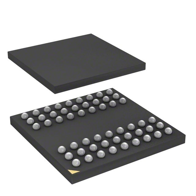
IC DRAM 256MBIT PAR 54TFBGA |
|---|---|
| Quantity | 1,155 Available (as of June 14, 2026) |

| Product Category | Memory |
|---|---|
| Manufacturer | Integrated Silicon Solution Inc |
| Manufacturing Status | Obsolete |
| Manufacturer Standard Lead Time | Contact Us |
| Datasheet |
Specifications & Environmental
| Device Package | 54-TFBGA (8x8) | Memory Format | DRAM | Technology | SDRAM | ||
|---|---|---|---|---|---|---|---|
| Memory Size | 256 Mbit | Access Time | 5.4 ns | Grade | Commercial | ||
| Clock Frequency | 143 MHz | Voltage | 3V ~ 3.6V | Memory Type | Volatile | ||
| Operating Temperature | 0°C ~ 70°C (TA) | Write Cycle Time Word Page | N/A | Packaging | 54-TFBGA | ||
| Mounting Method | Volatile | Memory Interface | Parallel | Memory Organization | 16M x 16 | ||
| Moisture Sensitivity Level | 3 (168 Hours) | RoHS Compliance | ROHS3 Compliant | REACH Compliance | REACH Unaffected | ||
| Qualification | N/A | ECCN | EAR99 | HTS Code | 8542.32.0024 |
Overview of IS42S16160G-7BL-TR – IC DRAM 256Mbit Parallel 54-TFBGA
The IS42S16160G-7BL-TR is a 256 Mbit synchronous DRAM organized as 16M × 16 with a parallel memory interface in a 54-ball TFBGA (8×8) package. The device implements a pipelined architecture with fully synchronous operation referenced to the rising edge of the clock.
Designed for systems that require a 256 Mbit SDRAM with programmable burst modes, selectable CAS latency and standard 3.3 V power, the device provides selectable timing and refresh options to match a variety of synchronous memory subsystems within the commercial 0°C to +70°C temperature range.
Key Features
- Memory Core The device is organized as 16M × 16 (256 Mbit) SDRAM with internal bank architecture (4 banks) for row access/precharge hiding.
- Timing & Performance Supports clock frequencies up to 143 MHz for the -7 timing option and access times of 5.4 ns from clock; programmable CAS latency of 2 or 3 clocks.
- Burst Control Programmable burst lengths (1, 2, 4, 8, full page) and selectable burst sequence (sequential or interleave) for flexible data transfer patterns.
- Refresh & Self-Maintenance Auto Refresh (CBR) and Self Refresh supported; 8K refresh cycles specified with 32 ms (A2) or 64 ms (commercial/A1/industrial) options as defined in the datasheet.
- Interface & Signaling LVTTL-compatible interface with all signals referenced to the positive clock edge for synchronous operation.
- Power Single power supply operation at 3.3 V nominal (3.0 V to 3.6 V supply range).
- Package & Temperature 54-ball TFBGA (8×8) package; commercial operating temperature 0°C to +70°C (TA) as specified.
Typical Applications
- Synchronous DRAM memory subsystems For system designs that require a 256 Mbit parallel SDRAM with programmable burst and CAS timing.
- Board-level embedded designs Fits applications that require a 54-ball TFBGA (8×8) footprint and 3.3 V supply within a 0°C to +70°C operating range.
- Buffered data storage and refresh management Suited to designs leveraging Auto Refresh and Self Refresh with internal bank architecture for efficient row management.
Unique Advantages
- Flexible timing configuration: Programmable CAS latency (2 or 3 clocks) and multiple burst lengths enable matching to system timing and throughput needs.
- Synchronous, pipelined architecture: All I/O referenced to the positive clock edge and pipeline operation support predictable, clocked transfers.
- Verified refresh options: Auto Refresh and Self Refresh modes with 8K refresh cycles specified for either 32 ms or 64 ms intervals provide selectable retention characteristics.
- Standard 3.3 V supply: Operates across a 3.0 V to 3.6 V range to align with common 3.3 V system rails.
- Compact BGA footprint: 54-ball TFBGA (8×8) package provides a board-space-efficient option for high-density memory placement.
Why Choose IS42S16160G-7BL-TR?
The IS42S16160G-7BL-TR offers a straightforward 256 Mbit synchronous DRAM solution with selectable timing, programmable burst modes and refresh control—features that help align memory behavior with host system requirements. Its 16M × 16 organisation, LVTTL interface and 54-ball TFBGA packaging make it suitable for designs needing a compact, parallel SDRAM device operating from a 3.3 V supply.
This device is well suited to engineers and procurement teams specifying a 256 Mbit SDRAM for systems that require defined timing options, refresh modes and a commercial temperature rating. The combination of synchronous operation, internal bank architecture and standard supply voltage supports scalable integration into existing memory subsystems.
For pricing, lead time or to request a quote for IS42S16160G-7BL-TR, submit a request with your required quantity and delivery details and our team will provide assistance.