IS42S16320B-7BLI
| Part Description |
IC DRAM 512MBIT PAR 54WBGA |
|---|---|
| Quantity | 885 Available (as of June 14, 2026) |

| Product Category | Memory |
|---|---|
| Manufacturer | Integrated Silicon Solution Inc |
| Manufacturing Status | Obsolete |
| Manufacturer Standard Lead Time | Contact Us |
| Datasheet |
Specifications & Environmental
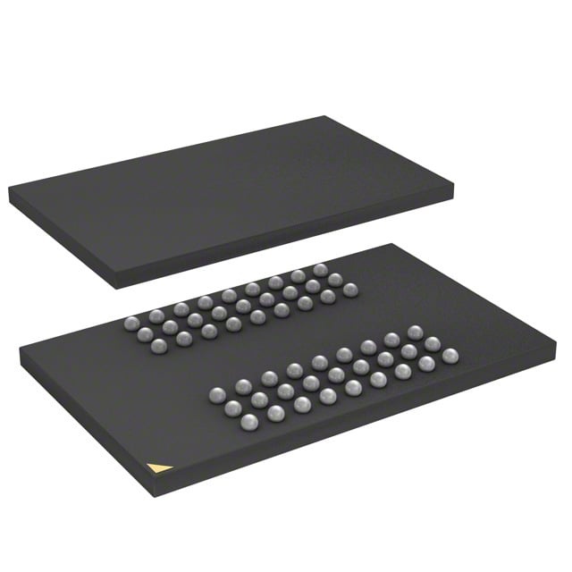
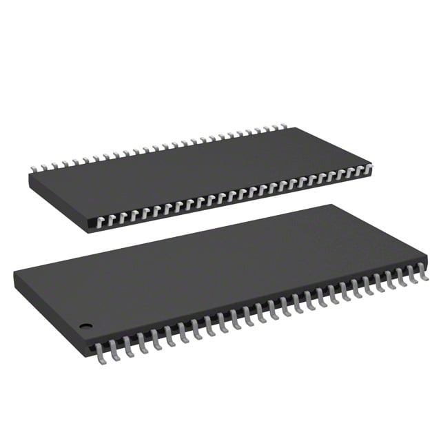
| Device Package | 54-WBGA (11x13) | Memory Format | DRAM | Technology | SDRAM | ||
|---|---|---|---|---|---|---|---|
| Memory Size | 512 Mbit | Access Time | 5.4 ns | Grade | Industrial | ||
| Clock Frequency | 143 MHz | Voltage | 3V ~ 3.6V | Memory Type | Volatile | ||
| Operating Temperature | -40°C ~ 85°C (TA) | Write Cycle Time Word Page | N/A | Packaging | 54-TFBGA | ||
| Mounting Method | Volatile | Memory Interface | Parallel | Memory Organization | 32M x 16 | ||
| Moisture Sensitivity Level | 3 (168 Hours) | RoHS Compliance | ROHS3 Compliant | REACH Compliance | REACH Unaffected | ||
| Qualification | N/A | ECCN | EAR99 | HTS Code | 8542.32.0028 |
Overview of IS42S16320B-7BLI – IC DRAM 512Mbit PAR 54WBGA
The IS42S16320B-7BLI is a 512Mbit synchronous DRAM organized as 32M × 16, implementing a pipelined architecture for high-speed data transfer. It is a fully synchronous parallel DRAM with internal banks, programmable burst operation and CAS latency options, designed for systems that require fast, temporary data storage and predictable clock-referenced operation.
This device supports clocked operation up to 143 MHz for the -7 speed grade, an access time of 5.4 ns (CAS latency = 3), and operates from a 3.0 V to 3.6 V supply. It is offered in a compact 54-ball W‑BGA (11 × 13) package and is specified for an extended operating temperature range of -40°C to +85°C (TA).
Key Features
- Core & Architecture Fully synchronous SDRAM with pipeline architecture and internal bank structure to optimize row access and precharge behavior.
- Memory Organization & Capacity 512 Mbit capacity organized as 32M × 16, providing wide parallel data paths for system memory buffering.
- Performance Clock frequency options include 166, 143 and 133 MHz (143 MHz for the -7 grade); access time of 5.4 ns at CAS latency = 3.
- Programmable Burst & Latency Programmable burst lengths (1, 2, 4, 8, full page) and burst sequences (sequential/interleave), with selectable CAS latency of 2 or 3 clocks.
- Refresh & Self-Refresh Auto Refresh (CBR) and Self Refresh supported; refresh options include 8K cycles per 16 ms (A2 grade) or 64 ms (Commercial/Industrial/A1 grades).
- Interface LVTTL-compatible interface with all signals referenced to the rising edge of the clock for deterministic timing.
- Power & Voltage Designed for VDD / VDDQ nominal 3.3 V operation with an allowable supply range of 3.0 V to 3.6 V.
- Package & Temperature Range Available in a 54-ball W‑BGA (11 × 13) package (54-TFBGA) and specified for operation from -40°C to +85°C (TA).
Typical Applications
- Embedded systems memory buffering Use as high-speed temporary storage in systems that require clocked synchronous access and burst transfers.
- High-throughput data buffers Suitable for designs needing wide parallel data paths (x16 organization) and programmable burst control for block transfers.
- Industrial electronics Operation to -40°C supports deployment in industrial temperature environments requiring reliable SDRAM performance.
Unique Advantages
- Deterministic synchronous operation: All signals referenced to the positive clock edge enable predictable timing and simplified system integration.
- Flexible burst control: Programmable burst lengths and sequences plus selectable CAS latency allow tuning for varied access patterns and throughput needs.
- Extended temperature support: Specified operation from -40°C to +85°C (TA) addresses temperature-demanding deployments.
- Compact, board-friendly package: 54-ball W‑BGA (11 × 13) provides a small footprint for space-constrained designs while offering x16 data width.
- Built-in refresh modes: Auto Refresh and Self Refresh with supported refresh-cycle options reduce external refresh management overhead.
- Standard 3.3 V signaling with flexible supply range: VDD/VDDQ nominal 3.3 V with an allowable 3.0 V to 3.6 V window for compatibility with common system power rails.
Why Choose IS42S16320B-7BLI?
The IS42S16320B-7BLI is positioned for designs that require a reliable, 512 Mbit synchronous DRAM with predictable, clock-referenced operation and flexible burst control. Its 32M × 16 organization, pipelined architecture and support for up to 143 MHz (–7) combine to deliver high-speed parallel data buffering in a compact 54-ball W‑BGA package.
This device is suitable for engineers specifying SDRAM for embedded and industrial systems that need selectable CAS latency, programmatic burst behavior, and built-in refresh management, all supported across an extended temperature range. The combination of performance, interface standardization, and package density provides long-term design scalability and integration simplicity.
If you need pricing, lead-time or availability details for IS42S16320B-7BLI, request a quote or submit an inquiry and our team will provide the information you need.