IS42S16320B-7TLI
| Part Description |
IC DRAM 512MBIT PAR 54TSOP II |
|---|---|
| Quantity | 506 Available (as of June 17, 2026) |

| Product Category | DRAM Memory |
|---|---|
| Manufacturer | Integrated Silicon Solution Inc |
| Manufacturing Status | Obsolete |
| Manufacturer Standard Lead Time | Contact Us |
| Datasheet |
Specifications & Environmental
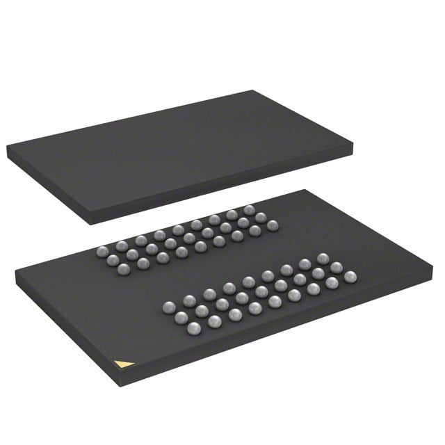
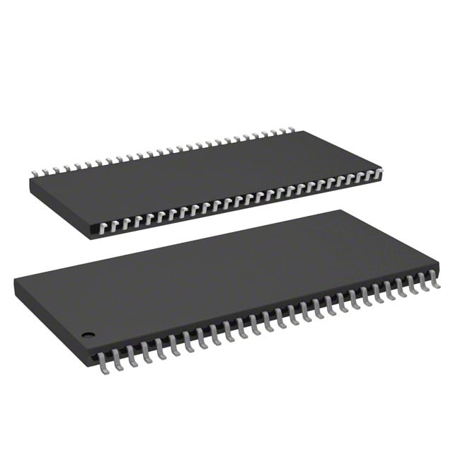
| Device Package | 54-TSOP II | Memory Format | DRAM | Technology | SDRAM | ||
|---|---|---|---|---|---|---|---|
| Memory Size | 512 Mbit | Access Time | 5.4 ns | Grade | Industrial | ||
| Clock Frequency | 143 MHz | Voltage | 3V ~ 3.6V | Memory Type | Volatile | ||
| Operating Temperature | -40°C ~ 85°C (TA) | Write Cycle Time Word Page | N/A | Packaging | 54-TSOP (0.400", 10.16mm Width) | ||
| Mounting Method | Volatile | Memory Interface | Parallel | Memory Organization | 32M x 16 | ||
| Moisture Sensitivity Level | 3 (168 Hours) | RoHS Compliance | ROHS3 Compliant | REACH Compliance | REACH Unaffected | ||
| Qualification | N/A | ECCN | EAR99 | HTS Code | 8542.32.0024 |
Overview of IS42S16320B-7TLI – IC DRAM 512MBIT PAR 54TSOP II
The IS42S16320B-7TLI is a 512 Mbit synchronous DRAM organized as 32M × 16 with a parallel memory interface. It implements a fully synchronous, pipelined architecture with internal banks to support high-speed, predictable data transfers for systems requiring parallel SDRAM memory.
Designed for applications that require 3.0–3.6 V operation and extended temperature performance, the device is offered in a 54-pin TSOP-II package and supports programmable burst modes, auto and self-refresh, and LVTTL signaling.
Key Features
- Memory Organization 32M × 16 organization delivering a total of 512 Mbit of synchronous DRAM capacity in a single 54‑TSOP II package.
- Synchronous Pipeline Architecture Fully synchronous operation with all signals referenced to a positive clock edge and internal bank structure for hidden row access/precharge.
- Performance Supported clock frequency up to 143 MHz for the -7 timing grade with an access time from clock of 5.4 ns (CAS latency = 3).
- Burst and Latency Options Programmable burst lengths (1, 2, 4, 8, full page) and burst sequences (sequential/interleave), with selectable CAS latency (2 or 3 clocks).
- Refresh and Power Auto Refresh and Self Refresh support with 8K refresh cycles (timing varies by grade); power supply range 3.0 V to 3.6 V compatible with 3.3 V systems.
- Interface Parallel memory interface with LVTTL signaling for compatibility with parallel bus architectures.
- Package and Temperature 54‑pin TSOP‑II package (0.400", 10.16 mm width) and operating temperature range of -40 °C to +85 °C (TA).
Typical Applications
- Industrial Systems Use as system DRAM where extended temperature range (-40 °C to +85 °C) and parallel SDRAM interface are required for reliable operation.
- Embedded Memory High-capacity parallel memory for embedded platforms that need 512 Mbit SDRAM with programmable burst modes and low-latency access.
- Buffering and High‑Speed Data Transfer Applications that benefit from the device’s pipeline architecture, internal bank operation, and 143 MHz clock grade for predictable high-speed transfers.
Unique Advantages
- Fixed 32M × 16 Organization: Simplifies memory mapping and board-level design by providing a consistent 512 Mbit x16 footprint in a single device.
- Programmable Burst Control: Flexible burst lengths and sequences enable optimization for both sequential and random access patterns, reducing controller complexity.
- Deterministic Timing: Fully synchronous operation with defined CAS latency options (2 or 3 clocks) and specified access times supports predictable system timing.
- Standard 3.3 V Compatibility: Operates within a 3.0–3.6 V range suitable for common 3.3 V memory subsystems.
- Robust Refresh Modes: Auto and self-refresh capabilities with supported refresh cycles help maintain data integrity across operating conditions.
- Compact TSOP‑II Packaging: 54‑pin TSOP‑II package provides a space-efficient footprint for board-level integration.
Why Choose IS42S16320B-7TLI?
The IS42S16320B-7TLI combines a 512 Mbit SDRAM capacity with a synchronous, pipelined, quad‑bank architecture to deliver predictable timing and high-throughput parallel memory access. Its programmable burst modes, selectable CAS latency, and standard 3.0–3.6 V supply make it suitable for designs that require flexible performance tuning and straightforward integration into 3.3 V memory subsystems.
This device is well-suited to engineers and system designers building embedded and industrial platforms that need compact, high-capacity parallel DRAM with extended temperature tolerance and mature SDRAM feature set (auto/self-refresh, burst control, LVTTL interface).
For pricing, availability, or to request a quote and technical support, please contact our sales team or request a formal quote through the channel provided by your procurement process.