IS42S16320B-7TL-TR
| Part Description |
IC DRAM 512MBIT PAR 54TSOP II |
|---|---|
| Quantity | 76 Available (as of June 15, 2026) |

| Product Category | Memory |
|---|---|
| Manufacturer | Integrated Silicon Solution Inc |
| Manufacturing Status | Obsolete |
| Manufacturer Standard Lead Time | Contact Us |
| Datasheet |
Specifications & Environmental
| Device Package | 54-TSOP II | Memory Format | DRAM | Technology | SDRAM | ||
|---|---|---|---|---|---|---|---|
| Memory Size | 512 Mbit | Access Time | 5.4 ns | Grade | Commercial | ||
| Clock Frequency | 143 MHz | Voltage | 3V ~ 3.6V | Memory Type | Volatile | ||
| Operating Temperature | 0°C ~ 70°C (TA) | Write Cycle Time Word Page | N/A | Packaging | 54-TSOP (0.400", 10.16mm Width) | ||
| Mounting Method | Volatile | Memory Interface | Parallel | Memory Organization | 32M x 16 | ||
| Moisture Sensitivity Level | 3 (168 Hours) | RoHS Compliance | ROHS3 Compliant | REACH Compliance | REACH Unaffected | ||
| Qualification | N/A | ECCN | EAR99 | HTS Code | 8542.32.0024 |
Overview of IS42S16320B-7TL-TR – 512Mbit SDRAM, 32M × 16, 54‑TSOP II
The IS42S16320B-7TL-TR is a 512Mbit synchronous DRAM device organized as 32M × 16 with a parallel memory interface. It implements a fully synchronous, pipelined architecture with an internal quad-bank structure and all signals referenced to the rising edge of the clock.
Designed for 3.3V memory systems (VDD/VDDQ = 3.3V) and a specified supply range of 3.0V to 3.6V, this device supports high-speed burst transfers and programmable timing to fit a range of synchronous memory applications.
Key Features
- Memory Core 512 Mbit SDRAM organized as 32M × 16 with quad-bank internal configuration for row access/precharge hiding.
- Performance Supports clock frequencies up to 143 MHz for the -7 speed grade, with an access time of 5.4 ns (CAS Latency = 3).
- Programmable Burst & Timing Programmable burst lengths (1, 2, 4, 8, full page) and burst sequence (Sequential/Interleave), plus programmable CAS latency options of 2 or 3 clock cycles.
- Refresh and Self-Refresh Auto Refresh (CBR) and Self Refresh supported; 8K refresh cycles are specified every 16 ms (A2 grade) or 64 ms (Commercial/Industrial/A1 grades) per datasheet details.
- Interface Parallel LVTTL interface with synchronous inputs/outputs referenced to clock rising edge, enabling predictable timing in synchronous memory systems.
- Power Specified for operation in a 3.0V–3.6V supply range; datasheet indicates operation in 3.3V VDD and VDDQ memory systems.
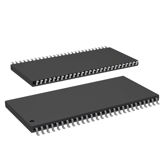
- Package & Temperature Supplied in a 54-pin TSOP‑II (0.400", 10.16 mm width) package. Commercial operating temperature range: 0°C to +70°C.
Typical Applications
- System Memory Use as parallel SDRAM system memory where 512 Mbit density and synchronous burst transfers are required.
- Buffering and Frame Storage Suitable for high-speed buffering or frame storage functions that benefit from programmable burst lengths and low access times.
- Embedded Platforms Integration into embedded designs that require a compact 54‑TSOP II package and 3.3V memory operation.
Unique Advantages
- High-density 16-bit Organization: 32M × 16 organization delivers 512 Mbit capacity in a single device for streamlined memory design.
- Synchronous, Pipelined Architecture: All signals referenced to the rising clock edge and internal quad-bank architecture help maintain deterministic timing and efficient row management.
- Flexible Burst and Latency Options: Programmable burst lengths and CAS latencies (2 or 3) allow tuning for different access patterns and system timing requirements.
- Standard 3.3V Compatibility: Device is specified for use in 3.3V memory systems with an operating supply range of 3.0V–3.6V, simplifying integration with common memory power rails.
- Compact TSOP-II Package: 54-pin TSOP-II packaging provides a small footprint while retaining x16 data width for board-level density.
- Refresh Modes Supported: Auto Refresh and Self Refresh support reduces external refresh management and supports low-activity retention modes.
Why Choose IS42S16320B-7TL-TR?
The IS42S16320B-7TL-TR positions itself as a reliable 512Mbit synchronous DRAM option for designs that require a compact x16 memory device with synchronous, burst-capable operation. Its programmable burst lengths, CAS latency options, and internal quad-bank architecture provide designers with timing flexibility and efficient row handling to match varied system requirements.
This device is appropriate for engineers and procurement teams specifying parallel SDRAM in 3.3V systems who need verified timing parameters (143 MHz option, 5.4 ns access time at CAS‑3) and a small-footprint 54‑pin TSOP‑II package.
If you require pricing, lead-time information, or a formal quote for IS42S16320B-7TL-TR, request a quote or submit a quote request referencing the part number and required quantities.