IS42S16320D-6BLI
| Part Description |
IC DRAM 512MBIT PAR 54TFBGA |
|---|---|
| Quantity | 306 Available (as of June 15, 2026) |

| Product Category | DRAM Memory |
|---|---|
| Manufacturer | Integrated Silicon Solution Inc |
| Manufacturing Status | Obsolete |
| Manufacturer Standard Lead Time | Contact Us |
| Datasheet |
Specifications & Environmental
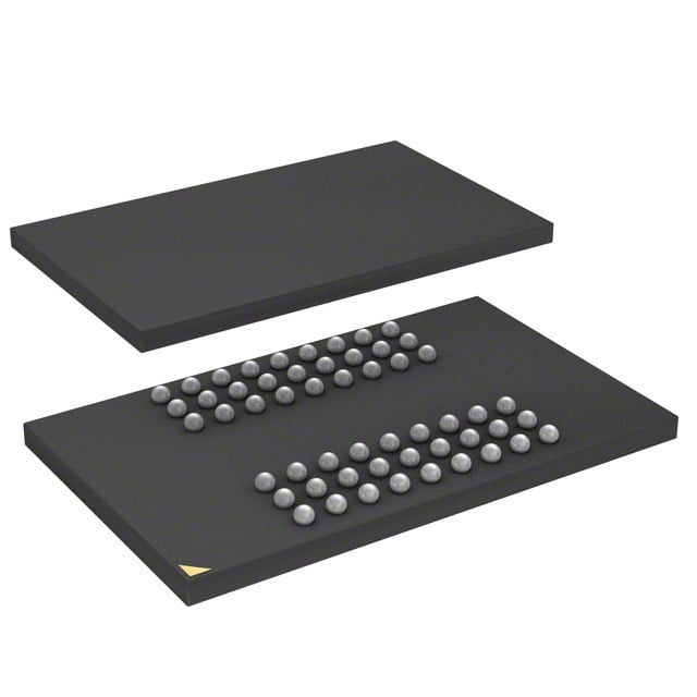
| Device Package | 54-TW-BGA (8x13) | Memory Format | DRAM | Technology | SDRAM | ||
|---|---|---|---|---|---|---|---|
| Memory Size | 512 Mbit | Access Time | 5.4 ns | Grade | Industrial | ||
| Clock Frequency | 166 MHz | Voltage | 3V ~ 3.6V | Memory Type | Volatile | ||
| Operating Temperature | -40°C ~ 85°C (TA) | Write Cycle Time Word Page | N/A | Packaging | 54-TFBGA | ||
| Mounting Method | Volatile | Memory Interface | Parallel | Memory Organization | 32M x 16 | ||
| Moisture Sensitivity Level | 3 (168 Hours) | RoHS Compliance | ROHS3 Compliant | REACH Compliance | REACH Unaffected | ||
| Qualification | N/A | ECCN | EAR99 | HTS Code | 8542.32.0028 |
Overview of IS42S16320D-6BLI – IC DRAM 512MBIT PAR 54TFBGA
The IS42S16320D-6BLI is a 512 Mbit synchronous DRAM organized as 32M × 16 with a parallel memory interface. It implements a fully synchronous pipeline architecture with internal bank management to support high-speed, burst-oriented memory transfers.
Designed for systems that require low-latency, high-throughput volatile memory, this device delivers predictable timing, programmable burst and CAS behavior, and an extended operating temperature range to support a variety of embedded and industrial designs.
Key Features
- Memory Core 512 Mbit SDRAM organized as 32M × 16 with internal bank architecture to hide row access/precharge and support efficient burst operations.
- Performance Clocked operation at 166 MHz (‑6 speed grade) with access time of 5.4 ns; programmable CAS latency (2 or 3 clocks) for flexible timing trade-offs.
- Burst and Sequencing Programmable burst lengths (1, 2, 4, 8, full page) and selectable burst sequences (sequential/interleave); supports burst read/write and burst read/single write modes with burst termination commands.
- Refresh and Power Management Auto Refresh and Self Refresh supported with 8K refresh cycles per 64 ms to maintain data integrity in volatile memory.
- Interface and Signaling Parallel memory interface with LVTTL signaling; all inputs and outputs referenced to the rising clock edge for synchronous operation.
- Power VDD/VDDQ supply range 3.0 V to 3.6 V, enabling integration into 3.x V power domains.
- Package and Mounting 54-ball TF-BGA (54-TF-BGA / supplier package 54-TW-BGA, 8×13); surface-mount BGA footprint for compact board-level integration.
- Temperature Range Industrial operating range from −40 °C to +85 °C (TA) for deployment in temperature-demanding environments.
- Reliability Features Internal bank precharge and timing programmability reduce access overhead and enable predictable, repeatable memory behavior.
Typical Applications
- Parallel memory subsystems For designs requiring a 512 Mbit parallel SDRAM device with deterministic synchronous timing and burst transfer capability.
- Industrial and embedded systems Suitable for embedded controllers and industrial electronics that need operation across −40 °C to +85 °C.
- High-throughput buffering Acts as buffer memory where programmable burst lengths and low access times (5.4 ns) improve sustained data transfer performance.
Unique Advantages
- Predictable synchronous timing: CAS latency programmability and clock-referenced I/O deliver repeatable, low-latency access patterns.
- Flexible burst control: Programmable burst lengths and sequences let designers optimize throughput and memory access patterns for application workloads.
- Wide operating voltage window: 3.0 V to 3.6 V supply range supports integration with common 3.x V systems.
- Industrial temperature capability: −40 °C to +85 °C rating accommodates temperature-sensitive deployments without added specification changes.
- Compact BGA footprint: 54-ball TF-BGA (8×13) provides a small board area for high-density system designs.
Why Choose IC DRAM 512MBIT PAR 54TFBGA?
The IS42S16320D-6BLI provides a balanced combination of synchronous performance, timing flexibility and industrial temperature tolerance for designs that require a 512 Mbit parallel SDRAM. Its internal bank management, programmable burst/CAS options and LVTTL interface enable deterministic behavior in burst-oriented data paths.
This device is well suited for engineers specifying board-level DRAM where compact packaging, predictable timing (166 MHz / 5.4 ns access), and support for auto/self-refresh are required. The straightforward electrical and timing characteristics make it a practical choice for scalable embedded and industrial memory subsystems.
Request a quote or submit a pricing inquiry to evaluate the IS42S16320D-6BLI for your next design or production program.