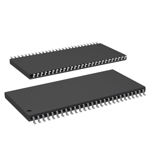
IS42S16320B-7TLI-TR
| Part Description |
IC DRAM 512MBIT PAR 54TSOP II |
|---|---|
| Quantity | 303 Available (as of June 15, 2026) |
| Product Category | Memory |
|---|---|
| Manufacturer | Integrated Silicon Solution Inc |
| Manufacturing Status | Obsolete |
| Manufacturer Standard Lead Time | Contact Us |
| Datasheet |
Specifications & Environmental
| Device Package | 54-TSOP II | Memory Format | DRAM | Technology | SDRAM | ||
|---|---|---|---|---|---|---|---|
| Memory Size | 512 Mbit | Access Time | 5.4 ns | Grade | Industrial | ||
| Clock Frequency | 143 MHz | Voltage | 3V ~ 3.6V | Memory Type | Volatile | ||
| Operating Temperature | -40°C ~ 85°C (TA) | Write Cycle Time Word Page | N/A | Packaging | 54-TSOP (0.400", 10.16mm Width) | ||
| Mounting Method | Volatile | Memory Interface | Parallel | Memory Organization | 32M x 16 | ||
| Moisture Sensitivity Level | 3 (168 Hours) | RoHS Compliance | ROHS3 Compliant | REACH Compliance | REACH Unaffected | ||
| Qualification | N/A | ECCN | EAR99 | HTS Code | 8542.32.0024 |
Overview of IS42S16320B-7TLI-TR – IC DRAM 512Mbit PAR 54TSOP II
The IS42S16320B-7TLI-TR is a 512Mbit synchronous DRAM organized as 32M × 16 with a parallel memory interface in a 54-pin TSOP-II package. It implements a pipelined, fully synchronous architecture with all signals referenced to the rising edge of the clock.
Designed for systems that require compact, board-level 512Mbit SDRAM, the device delivers high-speed operation (supported clock frequencies include 143 MHz for the -7 timing) with programmable CAS latency and built-in refresh modes to maintain data integrity across a wide operating temperature range.
Key Features
- Core / Architecture Quad-bank, pipelined synchronous DRAM architecture with all inputs/outputs referenced to the rising clock edge for deterministic timing.
- Memory 512 Mbit capacity organized as 32M × 16, providing parallel x16 data width for board-level memory expansion.
- Performance / Timing Supports clock frequencies including 143 MHz for the -7 device and programmable CAS latency (2 or 3 clocks). Access time from clock is 5.4 ns at CL = 3.
- Burst and Sequencing Programmable burst lengths (1, 2, 4, 8, full page) and selectable burst sequence (sequential or interleave) for flexible data transfer patterns.
- Refresh and Retention Auto Refresh (CBR) and Self Refresh supported; refresh options include 8K cycles per 16 ms (A2 grade) or per 64 ms (Commercial/Industrial/A1 grade) as defined in the device family.
- Interface / Logic Levels LVTTL-compatible interface for control signals and random column addressing every clock cycle for efficient column access.
- Power Operates from a 3.0 V to 3.6 V supply range (device family nominal 3.3 V VDD/VDDQ).
- Package & Mounting 54-pin TSOP-II package (0.400" / 10.16 mm width) optimized for compact board-level mounting.
- Temperature Range Rated for operation from -40 °C to +85 °C (TA), supporting designs that require an industrial temperature range.
Typical Applications
- Parallel memory subsystems Used where a 512Mbit parallel SDRAM device is required for board-level memory expansion or legacy parallel-memory interfaces.
- Compact board-level memory TSOP-II 54-pin package provides a dense form factor for space-constrained PCBs requiring x16 memory.
- Industrial temperature designs Suitable for systems that must operate across -40 °C to +85 °C ambient conditions.
Unique Advantages
- Deterministic synchronous operation: Fully synchronous design with all signals referenced to clock edge simplifies timing analysis and system integration.
- Configurable latency and burst modes: Programmable CAS latency and multiple burst length/sequence options enable tuning for throughput and access patterns.
- Built-in refresh management: Auto and self-refresh capability plus defined refresh cycles support stable data retention without external refresh logic.
- Wide supply tolerance: 3.0 V to 3.6 V operating range accommodates 3.3 V memory systems and board-level voltage variations.
- Industrial temperature support: Rated for -40 °C to +85 °C operation for reliable performance in temperature-sensitive deployments.
- Compact TSOP-II packaging: 54-pin TSOP-II (10.16 mm width) offers a small footprint for high-density memory implementations.
Why Choose IS42S16320B-7TLI-TR?
The IS42S16320B-7TLI-TR provides a straightforward, board-level 512Mbit SDRAM solution combining a x16 parallel interface, programmable timing/burst flexibility, and synchronous pipelined operation. Its specification set — including 143 MHz operation for the -7 timing, 5.4 ns access time at CL = 3, and industry-grade temperature range — makes it well-suited to designs that need compact, high-speed parallel DRAM in a TSOP-II footprint.
This device is appropriate for engineers and procurement teams seeking a verified 512Mbit SDRAM device with explicit timing, refresh options, and a narrow supply range for integration into existing 3.3 V memory systems.
Request a quote or submit a product inquiry to receive pricing and availability information for IS42S16320B-7TLI-TR.