IS42S16320D-7BL
| Part Description |
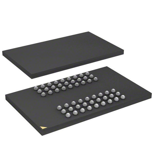
IC DRAM 512MBIT PAR 54TFBGA |
|---|---|
| Quantity | 1,486 Available (as of June 15, 2026) |

| Product Category | Memory |
|---|---|
| Manufacturer | Integrated Silicon Solution Inc |
| Manufacturing Status | Obsolete |
| Manufacturer Standard Lead Time | Contact Us |
| Datasheet |
Specifications & Environmental
| Device Package | 54-TW-BGA (8x13) | Memory Format | DRAM | Technology | SDRAM | ||
|---|---|---|---|---|---|---|---|
| Memory Size | 512 Mbit | Access Time | 5.4 ns | Grade | Commercial | ||
| Clock Frequency | 143 MHz | Voltage | 3V ~ 3.6V | Memory Type | Volatile | ||
| Operating Temperature | 0°C ~ 70°C (TA) | Write Cycle Time Word Page | N/A | Packaging | 54-TFBGA | ||
| Mounting Method | Volatile | Memory Interface | Parallel | Memory Organization | 32M x 16 | ||
| Moisture Sensitivity Level | 3 (168 Hours) | RoHS Compliance | ROHS Compliant | REACH Compliance | REACH Unaffected | ||
| Qualification | N/A | ECCN | EAR99 | HTS Code | 8542.32.0028 |
Overview of IS42S16320D-7BL – IC DRAM 512MBIT PAR 54TFBGA
The IS42S16320D-7BL is a 512Mbit synchronous DRAM organized as 32M × 16 with a parallel memory interface in a 54-ball TF-BGA package. It uses a pipelined, fully synchronous architecture with all signals referenced to the rising edge of the clock, delivering high-speed burst-capable memory for systems requiring fast, predictable access.
Designed for commercial temperature operation, the device supports programmable burst lengths and sequences, auto-refresh and self-refresh modes, and operates from a 3.0 V to 3.6 V supply range with a maximum clock frequency of 143 MHz for the -7 speed grade.
Key Features
- Memory Organization 512 Mbit DRAM arranged as 32M × 16 with internal banks to hide row access/precharge and support efficient memory banking.
- Performance Clock frequency up to 143 MHz (–7 grade) with an access time from clock of 5.4 ns (CAS latency options available), supporting low-latency burst operations.
- Synchronous Pipeline Architecture Fully synchronous operation with all inputs/outputs referenced to the rising clock edge and pipeline architecture for high-speed data transfer.
- Burst and Latency Options Programmable burst lengths (1, 2, 4, 8, full page) and selectable burst sequences (sequential/interleave); programmable CAS latency (2 or 3 clocks).
- Refresh and Reliability Auto Refresh and Self Refresh support with 8K refresh cycles every 64 ms to maintain data integrity.
- Interface and Signaling Parallel memory interface with LVTTL-compatible signaling and support for random column address every clock cycle.
- Power Power supply range 3.0 V to 3.6 V appropriate for the IS42S device family.
- Package and Temperature 54-TFBGA (54-ball TF-BGA, 8 × 13) package; commercial operating temperature 0°C to +70°C (TA).
Typical Applications
- High-speed system memory Used where synchronous, burst-capable DRAM is required for fast read/write buffering and throughput.
- Board-level memory expansion Provides a compact 512 Mbit solution in a 54-TFBGA footprint for space-constrained PCBs.
- Intermediate data buffering Supports burst read/write and burst read/single write operations for applications that leverage programmable burst sequences and lengths.
Unique Advantages
- Flexible burst control: Programmable burst lengths and selectable sequential or interleave burst sequences allow tuning for different access patterns.
- Low-latency operation: CAS latency options (2, 3 clocks) and a 5.4 ns access time from clock enable responsive memory access for time-sensitive functions.
- Synchronous pipelined design: All signals referenced to the clock edge and pipeline architecture deliver predictable timing for system integration.
- Refresh capability: Auto Refresh and Self Refresh modes with 8K/64 ms support reduce software refresh overhead and improve system reliability.
- Compact BGA package: 54-ball TF-BGA (8 × 13) provides a small footprint for dense board layouts while supporting x16 organization.
- Standard commercial range: Rated for 0°C to +70°C operation and a 3.0 V to 3.6 V supply range suitable for commercial designs.
Why Choose IC DRAM 512MBIT PAR 54TFBGA?
The IS42S16320D-7BL delivers a compact, synchronous 512 Mbit DRAM solution with configurable burst behavior, low access latency, and standard refresh features. Its pipelined architecture and LVTTL-compatible parallel interface make it suitable for designs that require predictable timing and high-throughput burst transfers.
This device is appropriate for commercial-temperature designs that need a 32M × 16 memory organization in a 54-TFBGA package, offering straightforward integration where density, burst flexibility, and synchronous operation are primary requirements.
Request a quote or submit an inquiry to receive pricing and availability information for the IS42S16320D-7BL.