IS42S16400F-6BL
| Part Description |
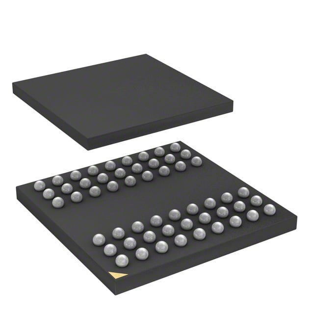
IC DRAM 64MBIT PARALLEL 54TFBGA |
|---|---|
| Quantity | 91 Available (as of June 10, 2026) |

| Product Category | Memory |
|---|---|
| Manufacturer | Integrated Silicon Solution Inc |
| Manufacturing Status | Obsolete |
| Manufacturer Standard Lead Time | Contact Us |
| Datasheet |
Specifications & Environmental
| Device Package | 54-TFBGA (8x8) | Memory Format | DRAM | Technology | SDRAM | ||
|---|---|---|---|---|---|---|---|
| Memory Size | 64 Mbit | Access Time | 5.4 ns | Grade | Commercial | ||
| Clock Frequency | 166 MHz | Voltage | 3V ~ 3.6V | Memory Type | Volatile | ||
| Operating Temperature | 0°C ~ 70°C (TA) | Write Cycle Time Word Page | N/A | Packaging | 54-TFBGA | ||
| Mounting Method | Volatile | Memory Interface | Parallel | Memory Organization | 4M x 16 | ||
| Moisture Sensitivity Level | 3 (168 Hours) | RoHS Compliance | ROHS3 Compliant | REACH Compliance | REACH Unaffected | ||
| Qualification | N/A | ECCN | EAR99 | HTS Code | 8542.32.0002 |
Overview of IS42S16400F-6BL – IC DRAM 64MBIT PARALLEL 54TFBGA
The IS42S16400F-6BL is a 64‑Mbit synchronous DRAM organized as 1,048,576 × 16 × 4 banks. It implements a fully synchronous pipeline architecture with all signals referenced to the rising edge of the clock.
Designed as a parallel LVTTL SDRAM device operating from a 3.0–3.6 V supply and 0°C to 70°C ambient, this device is suited for designs that require 64‑Mbit parallel memory with programmable burst control, internal bank management and standard SDRAM timing features.
Key Features
- Core / Memory Organization 64‑Mbit SDRAM arranged as 1M × 16 × 4 banks, providing a 16‑bit data path and internal bank architecture for improved access efficiency.
- Performance Supports a clock frequency of 166 MHz (device -6 timing) with an access time from clock of 5.4 ns (CAS latency = 3) and programmable CAS latency options (2 or 3 clocks).
- Interface Parallel LVTTL interface with random column addressing every clock cycle and support for burst read/write operations; programmable burst lengths (1, 2, 4, 8, full page) and burst sequence (sequential/interleave).
- Power Single 3.3 V power supply operation with specified voltage range of 3.0 V to 3.6 V.
- Timing & Refresh Self refresh and auto refresh (CBR) supported; standard refresh counts (4096 refresh cycles every 64 ms for commercial/industrial/A1 grades; A2 grade option available at 16 ms in datasheet).
- System Reliability Internal bank management hides row access/precharge and supports burst termination via burst stop and precharge commands.
- Package & Temperature 54‑ball TFBGA (8 mm × 8 mm) package; commercial operating temperature range 0°C to +70°C.
Typical Applications
- Embedded systems — Use as onboard parallel SDRAM where a 64‑Mbit, 16‑bit memory with programmable burst is required for system memory or buffering.
- High‑speed data buffers — Pipeline architecture and programmable burst lengths support burst read/write buffering in designs that require synchronous parallel SRAM alternatives.
- Digital equipment with parallel memory interfaces — Suitable for designs that rely on LVTTL parallel SDRAM interfacing and standard SDRAM control signals.
Unique Advantages
- Flexible burst control: Programmable burst lengths and sequence (sequential/interleave) allow tuning of memory transfer behavior to match system access patterns.
- Predictable timing: Programmable CAS latency (2 or 3) and documented access times (5.4 ns at CL=3) enable deterministic timing integration.
- Integrated bank management: Internal banking hides row access/precharge operations, simplifying timing considerations for row/column accesses.
- Simplified power design: Single 3.3 V supply operation (3.0–3.6 V range) reduces power-rail complexity in system designs.
- Compact ball‑grid package: 54‑TFBGA (8×8 mm) package provides a small footprint for space‑constrained PCB layouts.
Why Choose IS42S16400F-6BL?
The IS42S16400F-6BL delivers a compact 64‑Mbit synchronous DRAM solution with a 16‑bit data path and four internal banks for designs that need predictable SDRAM timing, programmable burst behavior and standard LVTTL parallel interfacing. Its documented timing parameters, refresh modes and single 3.3 V supply make it straightforward to integrate into systems with defined thermal and voltage envelopes.
This device is appropriate for engineers and procurement teams specifying parallel SDRAM with a 54‑TFBGA footprint and commercial temperature range, where stable timing, burst flexibility and a small package are priorities.
Request a quote or submit a product inquiry to obtain pricing, lead time and availability information for the IS42S16400F-6BL.