IS42S32160A-75BL
| Part Description |
IC DRAM 512MBIT PAR 90LFBGA |
|---|---|
| Quantity | 892 Available (as of June 14, 2026) |

| Product Category | Memory |
|---|---|
| Manufacturer | Integrated Silicon Solution Inc |
| Manufacturing Status | Obsolete |
| Manufacturer Standard Lead Time | Contact Us |
| Datasheet |
Specifications & Environmental
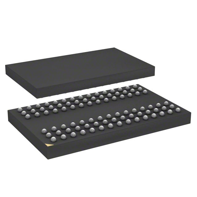
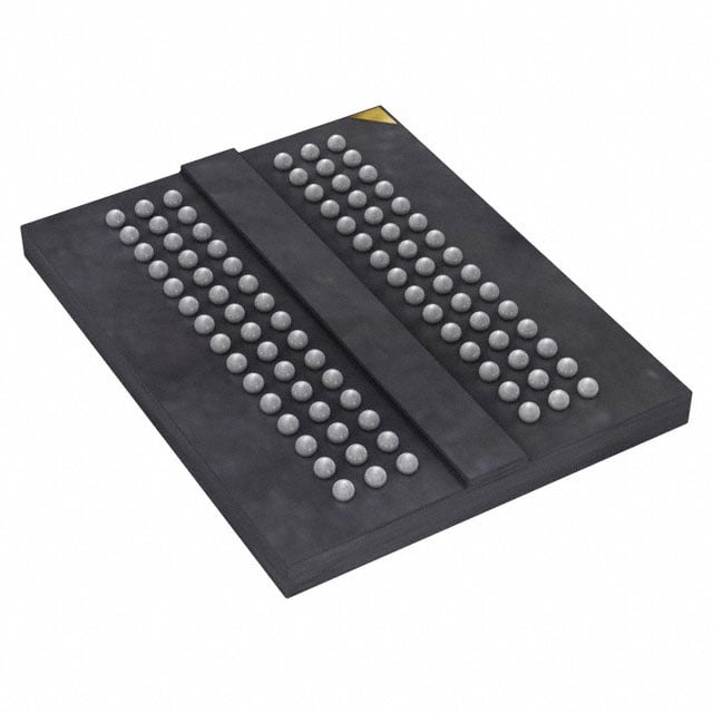
| Device Package | 90-LFBGA (8x13) | Memory Format | DRAM | Technology | SDRAM | ||
|---|---|---|---|---|---|---|---|
| Memory Size | 512 Mbit | Access Time | 6 ns | Grade | Commercial | ||
| Clock Frequency | 133 MHz | Voltage | 3V ~ 3.6V | Memory Type | Volatile | ||
| Operating Temperature | 0°C ~ 70°C (TA) | Write Cycle Time Word Page | N/A | Packaging | 90-LFBGA | ||
| Mounting Method | Volatile | Memory Interface | Parallel | Memory Organization | 16M x 32 | ||
| Moisture Sensitivity Level | 3 (168 Hours) | RoHS Compliance | ROHS3 Compliant | REACH Compliance | REACH Unaffected | ||
| Qualification | N/A | ECCN | EAR99 | HTS Code | 8542.32.0024 |
Overview of IS42S32160A-75BL – IC DRAM 512MBIT PAR 90LFBGA
The IS42S32160A-75BL from Integrated Silicon Solution Inc. (ISSI) is a 512‑Mbit synchronous DRAM device organized as 16M × 32 with four internal banks. It provides fully synchronous operation with a 133 MHz clock and a parallel LVTTL interface for deterministic, high‑speed memory transfers.
This device targets systems that require high memory bandwidth and flexible burst access, delivered in a compact 90‑ball LF‑BGA (8 × 13 mm) package with a single +3.3 V power supply (3.0–3.6 V operating range).
Key Features
- Core Architecture — Quad‑bank organization (4M × 32 × 4 banks) with internal pipelined architecture for sustained synchronous read/write operation.
- Memory Organization & Capacity — 16M × 32 configuration providing 512 Mbit total DRAM capacity.
- Speed & Timing — Clock rate up to 133 MHz and access time of 6 ns; selectable CAS latency of 2 or 3 for timing flexibility.
- Burst & Transfer Modes — Programmable burst lengths of 1, 2, 4, 8 or full‑page; supports interleaved or linear burst types and burst stop functionality.
- Data Masking & Byte Control — Individual byte control via DQM0–DQM3 to support partial‑word writes and masking.
- Refresh & Power Management — Auto Refresh and Self Refresh supported; standard refresh 8K cycles/64 ms (datasheet notes industrial option at 8K/32 ms).
- Interface & Supply — LVTTL input/output interface; single +3.3 V ±0.3 V supply (3.0–3.6 V).
- Package — 90‑ball LF‑BGA, 8 × 13 mm, 0.8 mm ball pitch; compact footprint for board‑space constrained designs. Pb‑free package option available per datasheet.
- Operating Range — Commercial temperature range listed at 0 °C to 70 °C (TA); datasheet also indicates availability in industrial temperature grades.
Typical Applications
- High‑bandwidth systems — Use where sustained high throughput and programmable burst behavior are required to support memory‑intensive tasks.
- Embedded memory subsystems — Suitable for designs needing a compact parallel SDRAM solution in a small LF‑BGA package.
- Performance‑sensitive designs — Systems that benefit from selectable CAS latency and internal pipelining for predictable timing and access patterns.
Unique Advantages
- Programmable burst control: Multiple burst lengths and burst types let designers optimize transfers for varying access patterns and throughput requirements.
- Quad‑bank architecture: Four internal banks improve concurrency and effective bandwidth for interleaved access scenarios.
- Compact LF‑BGA packaging: 90‑ball 8 × 13 mm package reduces PCB area while providing a high‑density DRAM solution.
- Flexible timing options: CAS latency selectable between 2 and 3 and a 133 MHz clock rate to balance latency and overall data rate.
- Standardized interface and supply: LVTTL signaling and single‑supply 3.3 V operation simplify integration with common system logic levels and power rails.
- Refresh and power modes: Auto and Self Refresh support enable simplified memory maintenance and low‑power standby behaviors when paired with clock enable control.
Why Choose IS42S32160A-75BL?
The IS42S32160A-75BL provides a synchronous, high‑bandwidth DRAM building block with programmable burst and latency options, a compact LF‑BGA footprint, and standard LVTTL interfacing. Its quad‑bank organization and internal pipelined architecture make it suitable for systems that need predictable, high‑throughput parallel memory access.
This device is appropriate for designs that require a 512‑Mbit SDRAM implemented in a small package with a single 3.3 V supply and commercial temperature operation; datasheet options include Pb‑free packaging and industrial temperature variants for projects that require those alternatives.
If you would like pricing, availability, or a formal quote for the IS42S32160A-75BL, please request a quote or contact sales for assistance.