IS42S32160B-6BLI
| Part Description |
IC DRAM 512MBIT PARALLEL 90WBGA |
|---|---|
| Quantity | 606 Available (as of June 15, 2026) |
| Product Category | Memory |
|---|---|
| Manufacturer | Integrated Silicon Solution Inc |
| Manufacturing Status | Obsolete |
| Manufacturer Standard Lead Time | Contact Us |
| Datasheet |
Specifications & Environmental
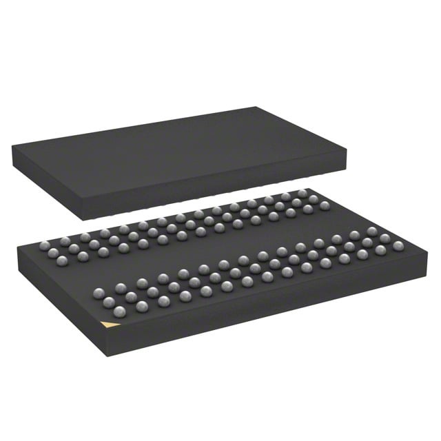
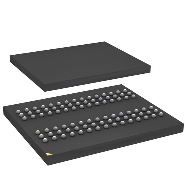
| Device Package | 90-WBGA (11x13) | Memory Format | DRAM | Technology | SDRAM | ||
|---|---|---|---|---|---|---|---|
| Memory Size | 512 Mbit | Access Time | 5.4 ns | Grade | Industrial | ||
| Clock Frequency | 166 MHz | Voltage | 3V ~ 3.6V | Memory Type | Volatile | ||
| Operating Temperature | -40°C ~ 85°C (TA) | Write Cycle Time Word Page | N/A | Packaging | 90-TFBGA | ||
| Mounting Method | Volatile | Memory Interface | Parallel | Memory Organization | 16M x 32 | ||
| Moisture Sensitivity Level | 3 (168 Hours) | RoHS Compliance | ROHS3 Compliant | REACH Compliance | REACH Unaffected | ||
| Qualification | N/A | ECCN | EAR99 | HTS Code | 8542.32.0028 |
Overview of IS42S32160B-6BLI – IC DRAM 512MBIT PARALLEL 90WBGA
The IS42S32160B-6BLI is a 512Mbit synchronous DRAM organized as 16M × 32 with a quad-bank internal architecture and a fully synchronous, LVTTL-referenced interface. It delivers high-speed pipeline transfers with programmable burst and CAS options in a compact 90-ball W‑BGA (11×13) package.
Designed for systems that require parallel synchronous DRAM at 3.3V operation, the device supports selectable burst lengths and refresh modes to balance throughput and power for embedded and board-level memory implementations.
Key Features
- Memory Organization 512 Mbit organized as 16M × 32 with 4 internal banks (4M × 32 × 4 banks) for interleaved access and improved throughput.
- High-Speed Synchronous Operation Clock-frequency support up to 166 MHz (CL = 3) with fully synchronous inputs and outputs referenced to the rising clock edge.
- Programmable Burst and CAS Programmable burst length (1, 2, 4, 8, full page) and burst sequence (sequential/interleave); selectable CAS latency of 2 or 3 clocks.
- Timing and Access Typical access time from clock is as low as 5.4 ns (CAS latency = 3) for fast read performance in burst operations.
- Refresh and Power Modes Auto Refresh (CBR) and Self Refresh supported with 8192 refresh cycles; refresh interval options include 16 ms (A2 grade) or 64 ms (Commercial/Industrial/A1 grade).
- Voltage and Interface Single power-supply operation at 3.3V ±0.3V (specified range 3.0V–3.6V) with an LVTTL-compatible parallel interface.
- Package and Temperature 90-ball W‑BGA (11×13) package; operating temperature range specified from −40°C to +85°C (TA).
Typical Applications
- 3.3V Memory Systems Acts as high-speed synchronous DRAM for systems designed around a 3.3V memory voltage domain.
- Board-Level DRAM Modules Used where compact WBGA footprint and quad-bank architecture are required for burst and interleaved memory access.
- Embedded High-Throughput Designs Suitable for designs that require pipeline synchronous transfers with programmable burst lengths and CAS latency options.
- Industrial-Temperature Electronics Applicable where operation across −40°C to +85°C is required.
Unique Advantages
- Flexible Burst Control: Programmable burst lengths and sequential/interleave sequencing allow tuning of transfer patterns to match system access behavior.
- Selectable CAS Latency: CAS latency options (2 or 3 clocks) provide trade-offs between clock rate and access timing to fit target system timing.
- Refresh Mode Options: Auto and Self Refresh with configurable refresh intervals (8K cycles per 16 ms or 64 ms depending on grade) support power-management strategies.
- Compact WBGA Package: 90-ball W‑BGA (11×13) enables denser board layouts while providing a package compatible with parallel SDRAM topologies.
- Wide Operating Range: Specified operation from −40°C to +85°C (TA) supports deployment in temperature-variable environments.
- LVTTL-Compatible Interface: Standard LVTTL signalling simplifies integration with systems using comparable logic levels.
Why Choose IS42S32160B-6BLI?
The IS42S32160B-6BLI combines a quad-bank, fully synchronous SDRAM architecture with programmable burst and CAS features to deliver configurable high-throughput memory in a compact WBGA package. Its 3.3V single-supply operation, LVTTL interface, and documented timing options make it suitable for board-level memory implementations that require deterministic, burst-oriented transfers.
This device is appropriate for engineers specifying parallel SDRAM where access timing, refresh behavior, and package density must be balanced against system design constraints. Documentation and device options (timing grades and temperature grades) enable selection aligned to performance and environmental requirements.
Request a quote or contact sales to discuss availability, lead times, and integration support for IS42S32160B-6BLI.