IS42S32160B-6TLI
| Part Description |
IC DRAM 512MBIT PAR 86TSOP II |
|---|---|
| Quantity | 1,081 Available (as of June 15, 2026) |

| Product Category | DRAM Memory |
|---|---|
| Manufacturer | Integrated Silicon Solution Inc |
| Manufacturing Status | Obsolete |
| Manufacturer Standard Lead Time | Contact Us |
| Datasheet |
Specifications & Environmental
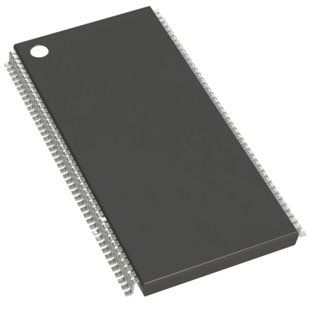
| Device Package | 86-TSOP II | Memory Format | DRAM | Technology | SDRAM | ||
|---|---|---|---|---|---|---|---|
| Memory Size | 512 Mbit | Access Time | 5.4 ns | Grade | Industrial | ||
| Clock Frequency | 166 MHz | Voltage | 3V ~ 3.6V | Memory Type | Volatile | ||
| Operating Temperature | -40°C ~ 85°C (TA) | Write Cycle Time Word Page | N/A | Packaging | 86-TFSOP (0.400", 10.16mm Width) | ||
| Mounting Method | Volatile | Memory Interface | Parallel | Memory Organization | 16M x 32 | ||
| Moisture Sensitivity Level | 3 (168 Hours) | RoHS Compliance | ROHS Compliant | REACH Compliance | REACH Unaffected | ||
| Qualification | N/A | ECCN | EAR99 | HTS Code | 8542.32.0028 |
Overview of IS42S32160B-6TLI – 512Mb Synchronous DRAM (86‑TSOP II)
The IS42S32160B-6TLI is a 512 Mbit synchronous DRAM organized as 16M × 32 with a quad-bank architecture and a fully synchronous interface. It implements pipeline transfer, programmable burst modes and internal bank interleaving to support high-rate, burst-oriented memory access patterns.
Supplied in an 86‑pin TSOP‑II package and specified for operation from -40°C to +85°C, this device targets systems that require high-speed parallel SDRAM with selectable CAS latency, flexible burst control, and standard LVTTL signaling.
Key Features
- Memory Capacity & Organization 512 Mbit density, organized as 16M × 32 with four internal banks (4M × 32 × 4 banks) for parallel, banked access.
- Synchronous SDRAM Architecture Fully synchronous operation with all signals referenced to the rising edge of CLK; supports LVTTL-compatible I/O.
- Clocking & Timing Supports up to 166 MHz clock frequency with programmable CAS latency (2 or 3 clocks). Typical access time from clock is 5.4 ns at CAS‑3.
- Burst Control Programmable burst lengths (1, 2, 4, 8, full page) and selectable burst sequence (sequential or interleave) with burst termination options.
- Refresh & Power Modes Auto Refresh (CBR) and Self Refresh supported; refresh cycles configurable per device grade (8192 cycles in 16 ms or 64 ms depending on grade).
- Power Single power supply operation with listed supply range of 3.0 V to 3.6 V (device specified nominally at 3.3 V ±0.3 V).
- Package & Mechanical 86‑TFSOP / 86‑TSOP II package (0.400", 10.16 mm width) optimized for compact board mounting.
- Operating Range Specified ambient operating temperature range: -40°C to +85°C (TA).
Typical Applications
- Embedded and Industrial Systems 512 Mbit of synchronous DRAM for embedded controllers and industrial electronics requiring -40°C to +85°C operation.
- High‑speed Buffers and Frame Memory Burst read/write and programmable burst lengths make the device suitable for designs that need predictable, high-rate data bursts and automatic column address generation.
- Networking and Communication Equipment Pipeline architecture and random column address capability every clock cycle support packet buffering and intermediary data storage in parallel memory subsystems.
Unique Advantages
- High throughput at 166 MHz: Supports up to 166 MHz clocking for low-latency synchronous transfers (CAS‑3 access time of 5.4 ns).
- Flexible memory timing: Programmable CAS latency (2 or 3 clocks) and multiple burst length/sequence options allow tuning for system timing and bandwidth requirements.
- Banked architecture for reduced latency: Four internal banks and internal precharge/bank interleave hide row access time and improve sustained access efficiency.
- Robust temperature range: Specified for -40°C to +85°C ambient operation to suit temperature-challenged deployments.
- Compact TSOP‑II package: 86‑pin TSOP‑II footprint provides a space-efficient solution for board-level memory integration.
- Low-power standby options: Auto refresh and self-refresh modes support power-saving operation during idle periods.
Why Choose IC DRAM 512MBIT PAR 86TSOP II?
The IS42S32160B-6TLI provides a balanced combination of high-speed synchronous operation, flexible burst and timing control, and a compact TSOP‑II package. Its quad-bank organization and pipeline architecture are suited to designs that require predictable burst performance and effective hiding of row access/precharge times.
This device is appropriate for engineers specifying parallel SDRAM in embedded, industrial, or high-throughput buffer applications where a 512 Mbit density, 3.0–3.6 V supply range, and -40°C to +85°C operation are required. Its configurable timing and refresh options support a range of system designs and operational modes.
Request a quote or submit a sales inquiry to obtain pricing, lead times and availability for the IS42S32160B-6TLI.