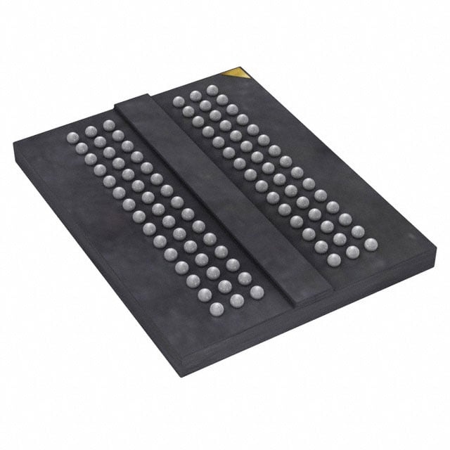
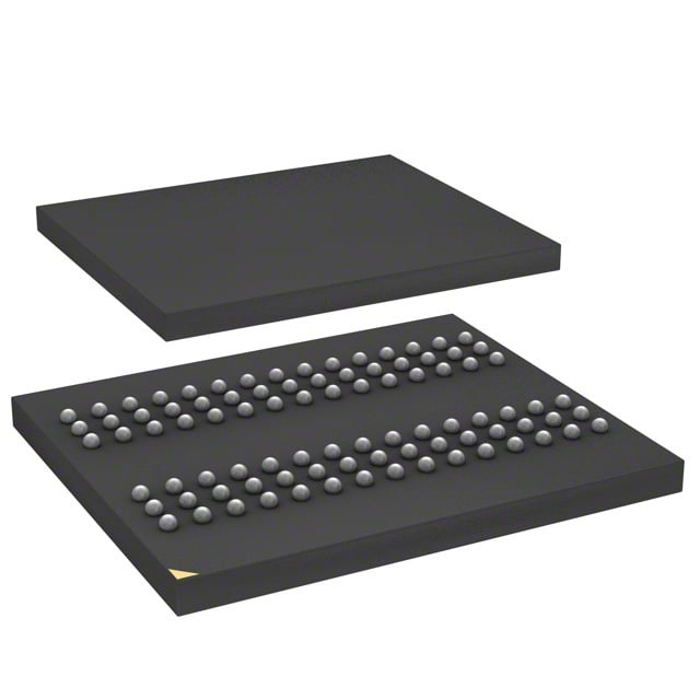
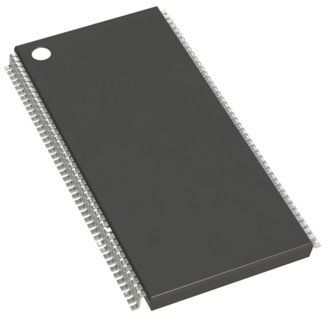
IS42S32160B-75ETLI
| Part Description |
IC DRAM 512MBIT PAR 86TSOP II |
|---|---|
| Quantity | 936 Available (as of June 18, 2026) |

| Product Category | DRAM Memory |
|---|---|
| Manufacturer | Integrated Silicon Solution Inc |
| Manufacturing Status | Obsolete |
| Manufacturer Standard Lead Time | Contact Us |
| Datasheet |
Specifications & Environmental
| Device Package | 86-TSOP II | Memory Format | DRAM | Technology | SDRAM | ||
|---|---|---|---|---|---|---|---|
| Memory Size | 512 Mbit | Access Time | 5.5 ns | Grade | Industrial | ||
| Clock Frequency | 133 MHz | Voltage | 3V ~ 3.6V | Memory Type | Volatile | ||
| Operating Temperature | -40°C ~ 85°C (TA) | Write Cycle Time Word Page | N/A | Packaging | 86-TFSOP (0.400", 10.16mm Width) | ||
| Mounting Method | Volatile | Memory Interface | Parallel | Memory Organization | 16M x 32 | ||
| Moisture Sensitivity Level | 3 (168 Hours) | RoHS Compliance | ROHS3 Compliant | REACH Compliance | REACH Unaffected | ||
| Qualification | N/A | ECCN | EAR99 | HTS Code | 8542.32.0028 |
Overview of IS42S32160B-75ETLI – IC DRAM 512MBIT PAR 86TSOP II
The IS42S32160B-75ETLI is a 512Mbit synchronous DRAM organized as 16M × 32 with a quad-bank architecture and a parallel LVTTL interface. It uses a pipelined synchronous architecture to support high-speed data transfer and programmable burst operations.
This device is intended for designs that require volatile SDRAM storage with a 3.0–3.6V supply, support for programmable CAS latency and burst sequencing, and industrial temperature operation to −40°C to +85°C.
Key Features
- Memory Architecture 512 Mbit SDRAM organized as 16M × 32 and implemented as 4M × 32 × 4 banks for internal bank interleaving and efficient row handling.
- Synchronous Pipeline Operation Fully synchronous operation with all signals referenced to the rising edge of CLK to enable predictable timing and pipeline data transfer.
- Clock and Timing Clock frequency rating of 133 MHz and access time down to 5.5 ns (device timing options include programmable CAS latency 2 or 3 as specified in the datasheet).
- Burst Control Programmable burst length (1, 2, 4, 8, full page) and selectable burst sequence (sequential or interleave) for flexible throughput patterns.
- Refresh and Power Modes Supports Auto Refresh (CBR) and Self Refresh; refresh options per datasheet include 8192 refresh cycles with selectable refresh timing options.
- Interface LVTTL-compatible signals and a parallel memory interface for direct integration into synchronous memory subsystems.
- Supply Voltage Operates from 3.0 V to 3.6 V (3.3 V ±0.3 V), compatible with standard 3.3 V memory systems.
- Package 86-pin TSOP II package (86-TFSOP, 0.400" / 10.16 mm width) optimized for surface-mount applications.
- Operating Temperature Industrial-range operation from −40°C to +85°C for use in temperature-demanding environments.
Typical Applications
- Embedded memory subsystems Used where high-speed, synchronous DRAM storage with programmable burst and CAS timing is required.
- Industrial control systems Suitable for systems that require operation across −40°C to +85°C and reliable refresh/self-refresh capabilities.
- Network and communications equipment Fits designs needing parallel SDRAM with low access times and bank interleaving to sustain data throughput.
- High-performance buffering Employed as a high-speed buffer or working memory where 512 Mbit capacity and 133 MHz clock operation are needed.
Unique Advantages
- Synchronous pipeline architecture: Enables consistent, clock-referenced data flow and predictable timing for system design.
- Flexible burst and CAS control: Programmable burst length and sequence plus selectable CAS latency allow tuning for throughput or latency needs.
- Quad-bank organization: Four internal banks provide the ability to hide row precharge time and support interleaved accesses for higher effective bandwidth.
- Industrial temperature range: −40°C to +85°C operation supports deployment in temperature-challenging environments.
- Standard 3.3 V supply range: 3.0–3.6 V operation ensures compatibility with common 3.3 V memory systems.
- Industry-standard TSOP II package: 86-pin TSOP-II package provides a compact surface-mount footprint for board-level integration.
Why Choose IS42S32160B-75ETLI?
The IS42S32160B-75ETLI delivers a 512 Mbit synchronous DRAM solution with programmable timing and burst features, a quad-bank architecture for internal interleaving, and LVTTL-compatible parallel interface—all in an 86-pin TSOP-II package. Its combination of 133 MHz rated operation, low access time, and flexible refresh modes makes it suitable for systems that require predictable, high-speed volatile memory behavior.
This device is well suited to engineers and procurement teams specifying SDRAM for embedded, industrial, and communication designs where 3.3 V supply compatibility, industrial temperature operation, and selectable timing/burst options are required. The device’s feature set supports scalable system integration and reliable runtime refresh control for sustained operation.
Request a quote or submit a procurement inquiry for IS42S32160B-75ETLI to receive pricing and availability information.