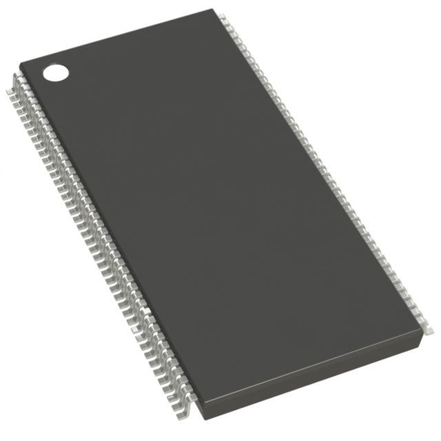
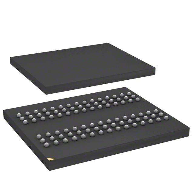
IS42S32160B-75TLI
| Part Description |
IC DRAM 512MBIT PAR 86TSOP II |
|---|---|
| Quantity | 883 Available (as of June 9, 2026) |

| Product Category | Memory |
|---|---|
| Manufacturer | Integrated Silicon Solution Inc |
| Manufacturing Status | Obsolete |
| Manufacturer Standard Lead Time | Contact Us |
| Datasheet |
Specifications & Environmental
| Device Package | 86-TSOP II | Memory Format | DRAM | Technology | SDRAM | ||
|---|---|---|---|---|---|---|---|
| Memory Size | 512 Mbit | Access Time | 5.5 ns | Grade | Industrial | ||
| Clock Frequency | 133 MHz | Voltage | 3V ~ 3.6V | Memory Type | Volatile | ||
| Operating Temperature | -40°C ~ 85°C (TA) | Write Cycle Time Word Page | N/A | Packaging | 86-TFSOP (0.400", 10.16mm Width) | ||
| Mounting Method | Volatile | Memory Interface | Parallel | Memory Organization | 16M x 32 | ||
| Moisture Sensitivity Level | 3 (168 Hours) | RoHS Compliance | ROHS3 Compliant | REACH Compliance | REACH Unaffected | ||
| Qualification | N/A | ECCN | EAR99 | HTS Code | 8542.32.0024 |
Overview of IS42S32160B-75TLI – IC DRAM 512Mbit PAR 86TSOP II
The IS42S32160B-75TLI is a 512 Mbit synchronous DRAM device organized as 16M × 32 with four internal banks. It implements a fully synchronous, pipelined architecture with programmable mode and burst operation for memory accesses.
Designed for systems requiring high memory bandwidth, the device supports up to 133 MHz clock operation, single +3.3 V ±0.3 V supply, and an industrial temperature option to address a range of embedded and bandwidth-sensitive designs.
Key Features
- Core Architecture Quad-bank organization: four internal banks arranged as 4M × 32 bits × 4 banks (16M × 32 total) to support interleaved access and improved throughput.
- Synchronous SDRAM Operation Fully synchronous operation with all inputs registered on the positive clock edge and an internal pipelined architecture for deterministic timing.
- Performance Clock rate support up to 133 MHz for the -75 option (device options include 133 and 143 MHz rates); CAS latency selectable at 2 or 3 with access time from clock as low as 5.4 ns.
- Burst and Mode Flexibility Programmable mode register, selectable burst lengths (1, 2, 4, 8, or full page), burst type (interleaved or linear) and burst stop functionality for flexible read/write patterns.
- Refresh and Power Auto Refresh and Self Refresh supported with 8K refresh cycles per 64 ms; single +3.3 V ±0.3 V power supply simplifies power rail design.
- Byte Masking and Interface Individual byte control via DQM0–DQM3 and LVTTL-compatible interface signaling for parallel data control.
- Package and Temperature Available in an 86-pin TSOP-II package (0.5 mm pin pitch, 10.16 mm width); temperature options include industrial range (−40°C to +85°C).
- Manufacturing Options Die revision B with package options including 86-pin TSOP-II and 90-ball BGA; lead-free package is available.
Typical Applications
- High-Bandwidth Embedded Systems Used where sustained data throughput is required; the device's quad-bank SDRAM architecture and burst modes support high-rate memory transfers.
- Memory-Intensive Processing Suitable for designs that benefit from programmable CAS latency and selectable burst lengths to tune latency and throughput.
- Industrial Temperature Designs The industrial temperature option (−40°C to +85°C) makes the device applicable for systems deployed in wider ambient conditions.
Unique Advantages
- Four-Bank Architecture: Enables concurrent bank operation and improved effective throughput for interleaved access patterns.
- Programmable Burst and Mode Control: Selectable burst lengths, burst type and programmable mode register let designers tailor memory behavior to application access patterns.
- Low-Latency Operation: CAS latency options (2 or 3) with 5.4 ns access-from-clock timing provide predictable, low-latency reads and writes.
- Standard 3.3 V Power: Single +3.3 V ±0.3 V supply eases integration into existing 3.3 V platforms.
- Robust Refresh Management: Auto and Self Refresh support with 8K/64 ms refresh cycles simplifies retention and low-power pause states.
- Industry-Standard Packaging: 86-pin TSOP-II (0.5 mm pitch) and BGA options allow flexible board-level mounting and density choices.
Why Choose IS42S32160B-75TLI?
The IS42S32160B-75TLI delivers a synchronous, pipelined SDRAM architecture that balances configurable latency and high throughput for designs that demand sustained memory performance. With selectable CAS latency, flexible burst modes, and four internal banks, it offers designers the control needed to optimize memory behavior for specific workloads.
This device is appropriate for customers building bandwidth-sensitive systems that require a 512 Mbit DRAM on a single +3.3 V rail and an industrial temperature option. Its package options and programmable features provide practical integration choices for embedded and high-throughput applications.
Request a quote or submit an inquiry for IS42S32160B-75TLI to obtain pricing, availability, and ordering information.