IS42S32160B-7BLI
| Part Description |
IC DRAM 512MBIT PAR 90LFBGA |
|---|---|
| Quantity | 1,228 Available (as of June 15, 2026) |
| Product Category | DRAM Memory |
|---|---|
| Manufacturer | Integrated Silicon Solution Inc |
| Manufacturing Status | Obsolete |
| Manufacturer Standard Lead Time | Contact Us |
| Datasheet |
Specifications & Environmental
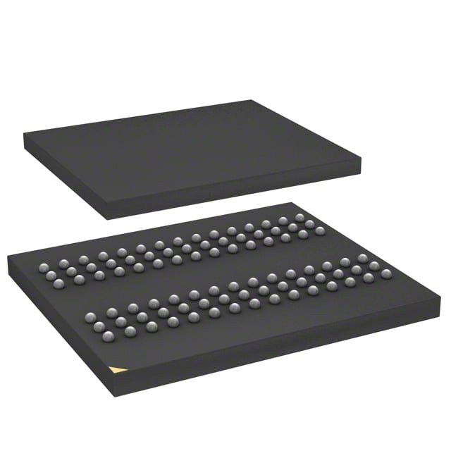
| Device Package | 90-LFBGA (13x11) | Memory Format | DRAM | Technology | SDRAM | ||
|---|---|---|---|---|---|---|---|
| Memory Size | 512 Mbit | Access Time | 5.4 ns | Grade | Industrial | ||
| Clock Frequency | 143 MHz | Voltage | 3V ~ 3.6V | Memory Type | Volatile | ||
| Operating Temperature | -40°C ~ 85°C (TA) | Write Cycle Time Word Page | N/A | Packaging | 90-LFBGA | ||
| Mounting Method | Volatile | Memory Interface | Parallel | Memory Organization | 16M x 32 | ||
| Moisture Sensitivity Level | 3 (168 Hours) | RoHS Compliance | ROHS3 Compliant | REACH Compliance | REACH Unaffected | ||
| Qualification | N/A | ECCN | EAR99 | HTS Code | 8542.32.0024 |
Overview of IS42S32160B-7BLI – IC DRAM 512MBIT PAR 90LFBGA
The IS42S32160B-7BLI is a 512Mbit synchronous DRAM (SDRAM) organized as 16M × 32 with a quad-bank architecture and pipeline operation. It is designed for synchronous parallel memory systems that require high‑speed burst transfers and predictable clock‑referenced timing.
All signals are referenced to the positive edge of the clock, the device operates from a single 3.3V ±0.3V supply (3.0V–3.6V), and it is available in a 90‑LFBGA (13×11) package with an operating temperature range of −40°C to 85°C (TA).
Key Features
- Core / Architecture Quad‑bank SDRAM with internal bank interleaving and pipeline architecture to support high‑speed data transfer and hide row access/precharge latency.
- Memory Organization 512 Mbit capacity arranged as 16M × 32 (4M × 32 × 4 banks).
- Performance Clock frequency up to 143 MHz (–7 speed grade) and access time from clock of 5.4 ns at CAS latency = 3.
- Programmable Burst and Latency Programmable burst lengths (1, 2, 4, 8, full page), selectable burst sequence (sequential/interleave), and programmable CAS latency (2 or 3 clocks) for performance tuning.
- Refresh and Power Modes Auto Refresh (CBR) and Self Refresh supported; refresh counts per datasheet include 8K cycles per 64 ms (Commercial/Industrial/A1) and 8K per 16 ms for A2 grade.
- Interface LVTTL compatible signals and parallel memory interface with random column address every clock cycle during burst operations.
- Burst Operations Supports burst read/write, burst read/single write and burst termination via burst stop and precharge command.
- Power Supply Single power supply: 3.3V ±0.3V (3.0V–3.6V).
- Package and Mounting 90‑LFBGA (90‑ball W‑BGA, 13×11) ball grid array package for surface mount applications.
- Operating Temperature Specified for −40°C to +85°C (TA).
Typical Applications
- System Memory Use as synchronous parallel DRAM in 3.3V memory subsystems requiring predictable clock‑referenced timing and burst transfers.
- Embedded Platforms Memory expansion for embedded systems that need 512Mbit SDRAM with selectable CAS latency and burst behavior.
- High‑Speed Buffering Buffering and temporary storage in designs that leverage burst read/write and random column access per clock cycle.
Unique Advantages
- Synchronous, clock‑referenced operation: Ensures all inputs and outputs are registered on the rising clock edge for deterministic timing.
- Flexible performance tuning: Programmable CAS latency and burst length/sequence allow tradeoffs between latency and throughput.
- Bank interleaving: Internal quad‑bank architecture hides row precharge and improves continuous data throughput during interleaved accesses.
- Broad supply tolerance: Single 3.3V supply range (3.0V–3.6V) aligns with standard 3.3V memory systems.
- Industrial temperature rating: Specified operation from −40°C to +85°C supports temperature‑sensitive applications.
- BGA package option: 90‑LFBGA (13×11) ball‑grid package for surface mount integration.
Why Choose IS42S32160B-7BLI?
The IS42S32160B-7BLI combines a 512Mbit SDRAM capacity with a synchronous, pipelined quad‑bank architecture to deliver configurable burst performance and predictable clock‑based timing. Its programmable CAS latency, burst length options, and LVTTL interface make it suitable for designs that require flexible performance tuning within 3.3V memory systems.
This device is suited for engineers specifying high‑speed parallel SDRAM in industrial temperature environments and for applications that require reliable burst read/write behavior, bank interleaving, and standard BGA mounting.
Request a quote or submit an RFQ for IS42S32160B-7BLI to check availability, pricing, and lead times for your procurement and design planning.