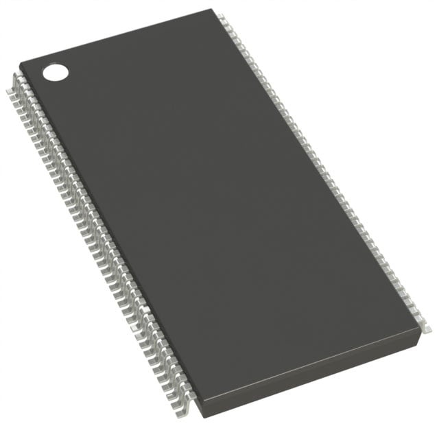
IS42S32160B-7TL-TR
| Part Description |
IC DRAM 512MBIT PAR 86TSOP II |
|---|---|
| Quantity | 222 Available (as of June 15, 2026) |

| Product Category | DRAM Memory |
|---|---|
| Manufacturer | Integrated Silicon Solution Inc |
| Manufacturing Status | Obsolete |
| Manufacturer Standard Lead Time | Contact Us |
| Datasheet |
Specifications & Environmental
| Device Package | 86-TSOP II | Memory Format | DRAM | Technology | SDRAM | ||
|---|---|---|---|---|---|---|---|
| Memory Size | 512 Mbit | Access Time | 5.4 ns | Grade | Commercial | ||
| Clock Frequency | 143 MHz | Voltage | 3V ~ 3.6V | Memory Type | Volatile | ||
| Operating Temperature | 0°C ~ 70°C (TA) | Write Cycle Time Word Page | N/A | Packaging | 86-TFSOP (0.400", 10.16mm Width) | ||
| Mounting Method | Volatile | Memory Interface | Parallel | Memory Organization | 16M x 32 | ||
| Moisture Sensitivity Level | 3 (168 Hours) | RoHS Compliance | ROHS Compliant | REACH Compliance | REACH Unaffected | ||
| Qualification | N/A | ECCN | EAR99 | HTS Code | 8542.32.0024 |
Overview of IS42S32160B-7TL-TR – IC DRAM 512MBIT PAR 86TSOP II
The IS42S32160B-7TL-TR is a 512Mbit synchronous DRAM device organized as 16M × 32 with an internal quad-bank architecture (4M × 32 × 4 banks). It implements a fully synchronous, pipeline architecture with all signals referenced to the rising edge of the clock.
Targeted for 3.3 V memory systems, this part delivers high-rate burst transfers with programmable burst length and sequence, programmable CAS latency, and support for Auto Refresh and Self Refresh modes—suited to systems that require synchronous, parallel DRAM with predictable timing and bank interleaving for hidden row access/precharge.
Key Features
- Memory Organization The device is 512Mbit organized as 16M × 32 with internal configuration of 4M × 32 × 4 banks for bank interleaving and precharge hiding.
- Synchronous SDRAM Core Fully synchronous operation with all signals referenced to the positive clock edge; LVTTL-compatible I/O.
- Speed and Timing Rated for a clock frequency of 143 MHz (‑7 speed grade) with an access time from clock of 5.4 ns at CAS Latency = 3; programmable CAS latency of 2 or 3 clocks.
- Burst Control Programmable burst length (1, 2, 4, 8, full page) and selectable burst sequence (sequential or interleave) with burst termination via burst stop or precharge.
- Refresh and Low-Power Modes Supports Auto Refresh and Self Refresh; 8192 refresh cycles with selectable refresh intervals (16 ms for A2 grade, 64 ms for Commercial/Industrial/A1 grades as specified).
- Voltage and Interface Single power supply operation at 3.3 V ±0.3 V (specified supply range 3.0 V to 3.6 V); parallel memory interface.
- Package and Temperature Offered in an 86-pin TSOP II (86‑TFSOP, 10.16 mm width) package and specified for commercial operating temperature range 0 °C to +70 °C.
- Column and Addressing Random column address capability every clock cycle; row addresses A0–A12, column addresses A0–A8, and bank address pins BA0/BA1.
Typical Applications
- 3.3 V Memory Subsystems For systems requiring a 512Mbit SDRAM organized as 16M × 32 with synchronous, parallel interface and LVTTL I/O.
- High‑rate Burst Buffering Suitable where synchronous burst transfers, programmable burst lengths, and bank interleaving are needed to sustain high data-rate bursts.
- Systems Requiring Self/Auto Refresh Applications that benefit from Auto Refresh and Self Refresh support with selectable refresh intervals.
Unique Advantages
- Deterministic synchronous operation: All inputs and outputs are referenced to the rising clock edge for predictable timing and easier system timing closure.
- Configurable latency and bursts: Programmable CAS latency (2 or 3 clocks) and flexible burst length/sequence settings enable tuning for different access patterns.
- Quad-bank architecture: Four internal banks with internal bank interleaving help hide row access/precharge times and improve sustained throughput for burst accesses.
- Industry-standard supply and interface: Single 3.3 V supply (3.0–3.6 V) and LVTTL-compatible interface simplify integration into existing 3.3 V memory systems.
- Commercial temperature and compact package: Commercial operating range (0 °C to +70 °C) in an 86-pin TSOP II package (10.16 mm width) for space-efficient board designs.
- Refresh flexibility: Multiple refresh interval options (including 8192 cycles across specified windows) to match system refresh requirements.
Why Choose IS42S32160B-7TL-TR?
The IS42S32160B-7TL-TR combines a 512Mbit synchronous DRAM architecture with programmable timing, burst control, and bank interleaving to deliver predictable, high-rate burst performance in a compact 86-pin TSOP II package. Its 3.3 V single-supply operation and LVTTL interface make it straightforward to integrate into standard 3.3 V memory subsystems.
This device is well suited for designs that require a synchronous, parallel DRAM with configurable latency and refresh behavior, offering adaptability across systems that need controlled timing, burst throughput, and compact packaging within a commercial temperature range.
Request a quote or submit a request for pricing and availability to evaluate the IS42S32160B-7TL-TR for your next design.