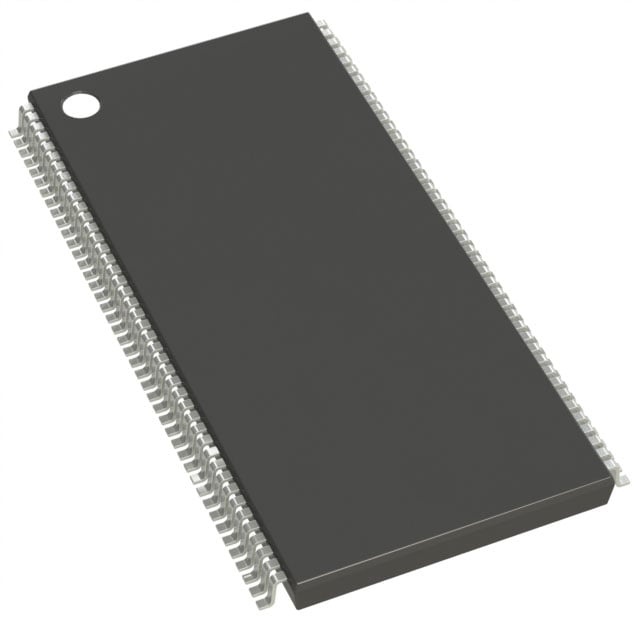
IS42S32160B-7TL
| Part Description |
IC DRAM 512MBIT PAR 86TSOP II |
|---|---|
| Quantity | 1,026 Available (as of June 18, 2026) |

| Product Category | DRAM Memory |
|---|---|
| Manufacturer | Integrated Silicon Solution Inc |
| Manufacturing Status | Obsolete |
| Manufacturer Standard Lead Time | Contact Us |
| Datasheet |
Specifications & Environmental
| Device Package | 86-TSOP II | Memory Format | DRAM | Technology | SDRAM | ||
|---|---|---|---|---|---|---|---|
| Memory Size | 512 Mbit | Access Time | 5.4 ns | Grade | Commercial | ||
| Clock Frequency | 143 MHz | Voltage | 3V ~ 3.6V | Memory Type | Volatile | ||
| Operating Temperature | 0°C ~ 70°C (TA) | Write Cycle Time Word Page | N/A | Packaging | 86-TFSOP (0.400", 10.16mm Width) | ||
| Mounting Method | Volatile | Memory Interface | Parallel | Memory Organization | 16M x 32 | ||
| Moisture Sensitivity Level | 3 (168 Hours) | RoHS Compliance | ROHS3 Compliant | REACH Compliance | REACH Unaffected | ||
| Qualification | N/A | ECCN | EAR99 | HTS Code | 8542.32.0024 |
Overview of IS42S32160B-7TL – IC DRAM 512MBIT PAR 86TSOP II
The IS42S32160B-7TL is a 512 Mbit synchronous DRAM (SDRAM) device organized as 16M × 32 with an internal quad-bank architecture and pipeline operation. It provides a fully synchronous, LVTTL-compatible parallel memory interface with registered inputs and outputs referenced to the rising edge of CLK.
Designed for commercial temperature-range systems, the device targets applications requiring high-speed parallel SDRAM in an 86‑TSOP II (0.400", 10.16 mm width) package, offering programmable burst modes, selectable CAS latency, and on-chip refresh options for reliable runtime operation.
Key Features
- Memory Core — 512 Mbit SDRAM organized as 16M × 32 (4M × 32 × 4 banks) to support wide, parallel data transfers and internal bank interleaving to hide row access/precharge time.
- Clock & Performance — Supports clock frequencies up to 143 MHz (–7 speed grade) with an access time from clock of 5.4 ns at CAS latency = 3; programmable CAS latency of 2 or 3 clocks.
- Burst and Access Modes — Programmable burst lengths (1, 2, 4, 8, full page) and burst sequence (sequential or interleave); burst read/write and burst read/single write capability with burst termination via stop or precharge command.
- Refresh & Power Management — Auto Refresh and Self Refresh supported; 8192 refresh cycles with timing options (e.g., 8K/64 ms for commercial grade) and a power-saving power-down mode.
- Interface — Parallel memory interface with LVTTL-compatible signals and the ability to present random column addresses every clock cycle during burst access.
- Supply & Temperature — Single 3.3 V power supply (operating range 3.0 V to 3.6 V) and commercial operating temperature range of 0°C to +70°C (TA).
- Package — Available in 86‑TSOP II (86‑TFSOP) package, 0.400" (10.16 mm) width, suitable for board-level mounting in space-conscious designs.
Typical Applications
- Commercial electronic systems — For designs operating within 0°C to +70°C that require 512 Mbit parallel SDRAM for high-speed data buffering and temporary storage.
- Board-level memory expansion — On‑board DRAM for systems needing a 16M × 32 memory organization in an 86‑TSOP II footprint.
- High-speed data buffering — Use where 143 MHz operation, programmable CAS latency and burst modes enable efficient burst read/write operations and random column access.
Unique Advantages
- Quad-bank architecture: Internal 4-bank organization and bank interleaving reduce effective latency by hiding precharge and row access time.
- Flexible burst control: Programmable burst lengths and sequence options allow designers to match memory throughput and access patterns to system requirements.
- Selectable CAS latency: CAS latency options (2 or 3 clocks) provide a balance between latency and maximum clock frequency for performance tuning.
- On-chip refresh and low-power modes: Auto Refresh, Self Refresh and power-down modes simplify refresh management and support power-sensitive designs.
- Standard supply and signaling: Single 3.3 V supply and LVTTL-compatible interface enable straightforward integration into common memory subsystem designs.
Why Choose IS42S32160B-7TL?
The IS42S32160B-7TL delivers a combination of high-speed synchronous operation and flexible memory control in a compact 86‑TSOP II package. With programmable CAS latency, multiple burst modes, and on-chip refresh features, it is well suited for commercial systems that demand predictable timing, wide parallel data paths, and board-level integration.
This device is appropriate for designers who require a 512 Mbit parallel SDRAM solution with explicit timing options (5.4 ns access from clock at CL=3, 143 MHz operation) and a standard 3.3 V supply window, providing a reliable component choice for memory subsystems in commercial temperature-range applications.
If you would like pricing, availability, or a formal quote for IS42S32160B-7TL, request a quote or contact the sales team to discuss options and lead times.