IS42S32160B-7BLI-TR
| Part Description |
IC DRAM 512MBIT PAR 90LFBGA |
|---|---|
| Quantity | 192 Available (as of June 18, 2026) |

| Product Category | DRAM Memory |
|---|---|
| Manufacturer | Integrated Silicon Solution Inc |
| Manufacturing Status | Obsolete |
| Manufacturer Standard Lead Time | Contact Us |
| Datasheet |
Specifications & Environmental
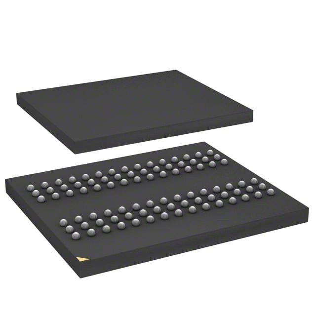
| Device Package | 90-LFBGA (13x11) | Memory Format | DRAM | Technology | SDRAM | ||
|---|---|---|---|---|---|---|---|
| Memory Size | 512 Mbit | Access Time | 5.4 ns | Grade | Industrial | ||
| Clock Frequency | 143 MHz | Voltage | 3V ~ 3.6V | Memory Type | Volatile | ||
| Operating Temperature | -40°C ~ 85°C (TA) | Write Cycle Time Word Page | N/A | Packaging | 90-LFBGA | ||
| Mounting Method | Volatile | Memory Interface | Parallel | Memory Organization | 16M x 32 | ||
| Moisture Sensitivity Level | 3 (168 Hours) | RoHS Compliance | ROHS3 Compliant | REACH Compliance | REACH Unaffected | ||
| Qualification | N/A | ECCN | EAR99 | HTS Code | 8542.32.0024 |
Overview of IS42S32160B-7BLI-TR – IC DRAM 512MBIT PAR 90LFBGA
The IS42S32160B-7BLI-TR is a 512 Mbit synchronous DRAM (SDRAM) organized as 16M × 32 with an internal quad-bank architecture. It provides pipelined, fully synchronous parallel memory access with programmable burst and CAS latency options for high-speed system buffering and data storage.
Designed for systems requiring a 3.3 V single-supply SDRAM solution with a 90‑ball LFBGA (13 × 11) package and an operating range of −40°C to 85°C, this device targets applications that need deterministic, clocked memory performance with refresh and power-saving modes.
Key Features
- Core / Memory Organization 512 Mbit SDRAM organized as 16M × 32 and internally as 4M × 32 × 4 banks for bank interleaving and efficient row/column operation.
- Clocked, Fully Synchronous Operation All signals referenced to the positive clock edge; specified for a 143 MHz clock frequency on the -7 variant to support high data-rate burst transfers.
- Programmable Burst and CAS Supports programmable burst length (1, 2, 4, 8, full page) and programmable burst sequence (sequential/interleave) with CAS latency options of 2 or 3 clocks.
- Performance Timing Access time from clock of 5.4 ns (CAS latency = 3) and random column address capability each clock cycle for continuous data flow during bursts.
- Refresh and Power Management Auto Refresh (CBR) and Self Refresh supported; refresh cycle counts documented (8,192 refresh cycles with A2 grade timing at 16 ms or commercial/industrial/A1 timing at 64 ms).
- Interface and Signaling LVTTL-compatible inputs/outputs and a parallel memory interface for integration into standard SDRAM memory controllers.
- Power Supply Single power supply operation at 3.3 V ±0.3 V (3.0 V to 3.6 V).
- Package and Temperature 90‑LFBGA (13 × 11) package; specified operating temperature range −40°C to 85°C (TA).
Typical Applications
- Parallel SDRAM memory expansion Provides 512 Mbit of volatile storage for systems that require synchronous, predictable parallel memory access.
- High-rate data buffering Used where burst transfers and random column access per clock are needed to sustain throughput during streaming or burst-oriented workloads.
- Embedded systems operating across temperature Suited for designs that require an SDRAM device with an industrial temperature range (−40°C to 85°C) and standard 3.3 V supply.
Unique Advantages
- Deterministic, clocked operation: Fully synchronous design with all signals referenced to the positive clock edge simplifies timing in clocked memory systems.
- Flexible burst control: Programmable burst lengths and sequences with programmable CAS latency enable tuning for throughput or latency in burst transfers.
- Quad-bank architecture: Internal banks and bank interleaving hide row access/precharge time to improve effective throughput during interleaved accesses.
- Robust refresh options: Auto and self-refresh modes with specified refresh counts provide predictable data retention and power management behavior.
- Standard power and signaling: 3.3 V single-supply operation and LVTTL-compatible I/O ease integration with common SDRAM controllers and legacy interfaces.
- Compact BGA package: 90‑ball LFBGA (13 × 11) enables high-density PCB layouts where board space is constrained.
Why Choose IS42S32160B-7BLI-TR?
The IS42S32160B-7BLI-TR combines a 512 Mbit SDRAM density with fully synchronous, pipelined architecture and programmable timing controls to meet designs that require predictable, high-rate parallel memory. Its quad-bank organization and support for burst/interleaved transfers help maximize sustained throughput in burst-oriented workloads.
This device is appropriate for engineers specifying a 3.3 V SDRAM with industrial temperature capability and a compact 90‑LFBGA footprint, offering configurable latency and refresh behaviors to match system timing and power requirements.
Request a quote or submit an inquiry to discuss availability, pricing, and lead times for the IS42S32160B-7BLI-TR.