IS42S32800D-6TLI-TR
| Part Description |
IC DRAM 256MBIT PAR 86TSOP II |
|---|---|
| Quantity | 350 Available (as of June 15, 2026) |
| Product Category | Memory |
|---|---|
| Manufacturer | Integrated Silicon Solution Inc |
| Manufacturing Status | Obsolete |
| Manufacturer Standard Lead Time | Contact Us |
| Datasheet |
Specifications & Environmental
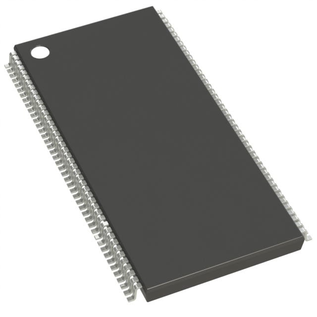
| Device Package | 86-TSOP II | Memory Format | DRAM | Technology | SDRAM | ||
|---|---|---|---|---|---|---|---|
| Memory Size | 256 Mbit | Access Time | 5.4 ns | Grade | Industrial | ||
| Clock Frequency | 166 MHz | Voltage | 3V ~ 3.6V | Memory Type | Volatile | ||
| Operating Temperature | -40°C ~ 85°C (TA) | Write Cycle Time Word Page | N/A | Packaging | 86-TFSOP (0.400", 10.16mm Width) | ||
| Mounting Method | Volatile | Memory Interface | Parallel | Memory Organization | 8M x 32 | ||
| Moisture Sensitivity Level | 3 (168 Hours) | RoHS Compliance | ROHS Compliant | REACH Compliance | REACH Unaffected | ||
| Qualification | N/A | ECCN | EAR99 | HTS Code | 8542.32.0024 |
Overview of IS42S32800D-6TLI-TR – 256Mbit Synchronous DRAM (86‑TSOP II)
The IS42S32800D-6TLI-TR is a 256Mbit synchronous DRAM organized as 8M × 32 and internally configured as 2M × 32 × 4 banks. It implements a pipelined, fully synchronous architecture with all signals referenced to the rising edge of the clock to support high-rate, predictable data transfers.
Designed for 3.0–3.6 V memory systems and LVTTL signaling, this 86‑pin TSOP‑II packaged device delivers selectable CAS latency and programmable burst options to suit systems requiring parallel SDRAM with up to 166 MHz clock operation and access times as low as 5.4 ns (CAS‑3).
Key Features
- Memory Organization 256 Mbit capacity arranged as 8M × 32 (2M × 32 × 4 banks), providing a parallel interface with quad‑bank architecture for interleaved access.
- Synchronous Pipeline Architecture Fully synchronous operation with all inputs and outputs registered on the positive clock edge to enable deterministic timing and high‑speed burst transfers.
- Performance Supports clock frequencies up to 166 MHz (CAS latency = 3) with access time from clock down to 5.4 ns (CAS‑3) for low‑latency read operations.
- Programmable Burst and CAS Programmable burst lengths (1, 2, 4, 8, full page) and burst sequence (sequential/interleave), plus selectable CAS latency of 2 or 3 clocks.
- Refresh and Power‑Saving Modes Auto Refresh and Self Refresh supported; refresh rate options specified (4K refresh cycles with commercial/industrial/A1/A2 grade timing variants documented in device specification).
- Interface and Logic Levels LVTTL compatible inputs and parallel memory interface for direct integration into standard 3.3 V memory subsystems.
- Supply Voltage Operates from 3.0 V to 3.6 V supply range.
- Package and Mounting Available in 86‑pin TSOP‑II (86‑TFSOP, 0.400", 10.16 mm width) surface‑mount package suitable for compact board layouts.
- Operating Temperature Specified to operate from −40 °C to +85 °C (TA) for extended environmental range.
Typical Applications
- 3.3 V Memory Subsystems Acts as parallel SDRAM for systems designed around a 3.0–3.6 V supply and LVTTL signaling.
- High‑Rate Data Buffers Used where burst transfers and low CAS latency (2 or 3 clocks) are required to support high‑throughput read/write operations.
- Compact Board Designs Suited for designs requiring a 256 Mbit SDRAM in an 86‑pin TSOP‑II footprint to conserve PCB area.
Unique Advantages
- Quad‑Bank Architecture: Internal four‑bank organization enables bank interleaving to hide row precharge and improve effective throughput.
- Flexible Burst Control: Programmable burst lengths and sequences allow optimization of sequential or random access patterns for system‑level performance tuning.
- Selectable CAS Latency: CAS latency options (2 or 3) provide designers tradeoffs between maximum clock rate and access timing to match system timing constraints.
- Robust Timing Documentation: Key timing parameters and access times (e.g., 5.4 ns at CAS‑3, 166 MHz operation) are specified to support accurate timing closure.
- Wide Operating Range: 3.0–3.6 V supply range and −40 °C to +85 °C operating temperature support a variety of 3.3 V system environments.
Why Choose IC DRAM 256MBIT PAR 86TSOP II?
The IS42S32800D-6TLI-TR delivers a well‑documented, fully synchronous 256 Mbit SDRAM solution for designs that require parallel DRAM with programmable burst behavior, selectable CAS latency, and predictable timing at up to 166 MHz. Its quad‑bank organization and pipeline architecture provide the mechanisms needed to optimize throughput in systems with high‑rate read/write requirements.
This device is suitable for engineers specifying a compact TSOP‑II packaged 3.3 V SDRAM with clear timing and refresh modes; it offers practical configurability for integration into memory subsystems where controlled latency, burst options, and standard LVTTL interfacing are important.
Request a quote or contact sales to discuss availability, pricing, and lead time for IS42S32800D-6TLI-TR.