IS42S32800D-75EB-TR
| Part Description |
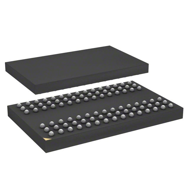
IC DRAM 256MBIT PAR 90TFBGA |
|---|---|
| Quantity | 343 Available (as of June 15, 2026) |

| Product Category | DRAM Memory |
|---|---|
| Manufacturer | Integrated Silicon Solution Inc |
| Manufacturing Status | Obsolete |
| Manufacturer Standard Lead Time | Contact Us |
| Datasheet |
Specifications & Environmental
| Device Package | 90-TFBGA (8x13) | Memory Format | DRAM | Technology | SDRAM | ||
|---|---|---|---|---|---|---|---|
| Memory Size | 256 Mbit | Access Time | 5.5 ns | Grade | Commercial | ||
| Clock Frequency | 133 MHz | Voltage | 3V ~ 3.6V | Memory Type | Volatile | ||
| Operating Temperature | 0°C ~ 70°C (TA) | Write Cycle Time Word Page | N/A | Packaging | 90-TFBGA | ||
| Mounting Method | Volatile | Memory Interface | Parallel | Memory Organization | 8M x 32 | ||
| Moisture Sensitivity Level | 3 (168 Hours) | RoHS Compliance | ROHS3 Compliant | REACH Compliance | REACH Unaffected | ||
| Qualification | N/A | ECCN | EAR99 | HTS Code | 8542.32.0002 |
Overview of IS42S32800D-75EB-TR – IC DRAM 256MBIT PAR 90TFBGA
The IS42S32800D-75EB-TR is a 256 Mbit synchronous DRAM organized as 8M × 32 with an internal quad-bank architecture (2M × 32 × 4 banks). It is a high-speed, fully synchronous parallel memory device optimized for systems requiring a 3.3 V supply and a LVTTL-compatible interface.
Designed for commercial temperature operation (0°C to +70°C) and supplied in a compact 90‑ball TF‑BGA (8×13) package, this device targets applications that need predictable burst access, programmable CAS latency, and standard refresh management for robust memory performance.
Key Features
- Core / Memory Organization 256 Mbit SDRAM organized as 8M × 32 (2M × 32 × 4 banks) for quadded-bank operation and internal row/bank management.
- Performance Clock frequency support up to 133 MHz for the -75E timing grade and an access time of 5.5 ns (CAS latency = 2, -75E variant).
- Programmable Burst & CAS Programmable burst lengths (1, 2, 4, 8, full page) and programmable burst sequence (sequential/interleave) with CAS latency options of 2 or 3 clocks.
- Refresh & Power Modes Auto Refresh and Self Refresh supported; commercial refresh rate of 4,096 cycles per 64 ms. Includes power-down and auto-precharge options.
- Interface & Signalling Fully synchronous operation with all signals referenced to the rising clock edge; LVTTL-compatible inputs and outputs for standard parallel system integration.
- Supply & Electrical Single-supply operation at 3.3 V ±0.3 V (specified 3.0 V to 3.6 V).
- Package & Mounting 90‑TFBGA (8×13) ball-grid package for compact board-level mounting.
- Operating Temperature Commercial grade operation: 0°C to +70°C (TA).
Typical Applications
- Embedded Systems Use as system memory where a compact 90‑TFBGA package and 256 Mbit volatile storage are required for program data buffering and working memory.
- Networking & Communications High-speed synchronous burst access and programmable CAS latency provide predictable throughput for packet buffering and temporary data queues.
- Consumer Electronics Suitable for devices that require low-latency parallel DRAM for frame buffers, image buffers or intermediate data storage at 3.3 V supply.
Unique Advantages
- Synchronous Quad‑Bank Architecture: Internal 4-bank organization (2M × 32 × 4) enables bank interleaving and reduced effective row precharge latency.
- Flexible Burst Control: Programmable burst lengths and sequential/interleave burst sequences adapt to varying data transfer patterns and system requirements.
- Programmable CAS Latency: Selectable CAS = 2 or 3 provides a trade-off between throughput and timing compatibility with host controllers.
- Standard Voltage & Signalling: 3.3 V single-supply operation and LVTTL-compatible I/O simplify integration into common legacy and contemporary 3.3 V systems.
- Compact TF‑BGA Package: 90-ball TF‑BGA (8×13) offers a small board footprint for space-constrained designs while supporting BGA assembly.
- Commercial Grade Refresh Support: 4,096 refresh cycles every 64 ms for commercial operation ensure data retention consistent with standard SDRAM refresh practices.
Why Choose IS42S32800D-75EB-TR?
The IS42S32800D-75EB-TR delivers a balanced combination of synchronous DRAM performance and packaging density for commercial 3.3 V systems. Its quad-bank architecture, programmable burst features, and selectable CAS latency make it suitable for designs that require predictable parallel memory access and timing flexibility.
This device is appropriate for engineers specifying 256 Mbit SDRAM in embedded, consumer, or networking equipment where compact TF‑BGA packaging and standard LVTTL interfacing simplify board-level integration and BOM alignment.
Request a quote or submit a product inquiry to receive pricing, availability, and lead-time information for IS42S32800D-75EB-TR.