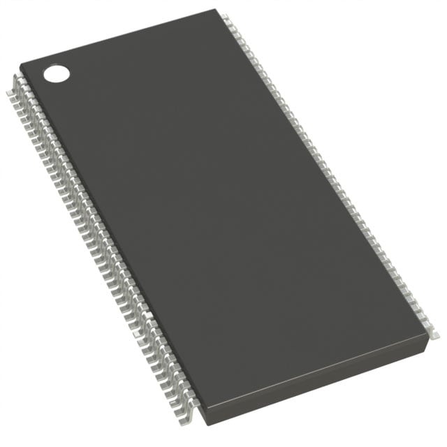
IS42S32800D-6TLI
| Part Description |
IC DRAM 256MBIT PAR 86TSOP II |
|---|---|
| Quantity | 293 Available (as of June 12, 2026) |

| Product Category | Memory |
|---|---|
| Manufacturer | Integrated Silicon Solution Inc |
| Manufacturing Status | Obsolete |
| Manufacturer Standard Lead Time | Contact Us |
| Datasheet |
Specifications & Environmental
| Device Package | 86-TSOP II | Memory Format | DRAM | Technology | SDRAM | ||
|---|---|---|---|---|---|---|---|
| Memory Size | 256 Mbit | Access Time | 5.4 ns | Grade | Industrial | ||
| Clock Frequency | 166 MHz | Voltage | 3V ~ 3.6V | Memory Type | Volatile | ||
| Operating Temperature | -40°C ~ 85°C (TA) | Write Cycle Time Word Page | N/A | Packaging | 86-TFSOP (0.400", 10.16mm Width) | ||
| Mounting Method | Volatile | Memory Interface | Parallel | Memory Organization | 8M x 32 | ||
| Moisture Sensitivity Level | 3 (168 Hours) | RoHS Compliance | ROHS Compliant | REACH Compliance | REACH Unaffected | ||
| Qualification | N/A | ECCN | EAR99 | HTS Code | 8542.32.0024 |
Overview of IS42S32800D-6TLI – IC DRAM 256MBIT PAR 86TSOP II
The IS42S32800D-6TLI is a 256Mbit synchronous DRAM organized as 8M × 32 with an internal quad-bank architecture and a parallel memory interface. It implements a fully synchronous, pipelined design with all signals referenced to the rising edge of the clock to support high-speed burst transfers in 3.3V memory systems.
This device is suited for systems requiring low-latency, high-throughput volatile storage in a compact 86-pin TSOP-II package and supports commercial and industrial operating ranges.
Key Features
- Memory Core The device is 256Mbit SDRAM organized as 8M × 32 (2M × 32 × 4 banks) to provide wide, parallel data paths and internal bank interleaving.
- Synchronous, High-Speed Interface Fully synchronous operation with a clock frequency up to 166 MHz (‑6 speed grade) and LVTTL-compatible I/O referencing the positive clock edge.
- Low Access Time Access time from clock of 5.4 ns at CAS Latency = 3 (‑6 grade), enabling tight read latency for time-sensitive bursts.
- Programmable Timing & Burst Control Programmable CAS latency (2 or 3 clocks), selectable burst lengths (1, 2, 4, 8, full page) and burst sequence (Sequential/Interleave) for flexible data-transfer patterns.
- Power Single power supply operation at 3.3V ±0.3V (3.0–3.6V) for standard 3.3V memory systems.
- Refresh & Power Management Auto Refresh and Self Refresh modes with 4096 refresh cycles; refresh interval options include 16 ms (A2 grade) or 64 ms (Commercial, Industrial, A1 grade).
- Banking & Throughput Internal bank structure and bank interleaving hide row access/precharge latency to improve effective throughput during burst operations.
- Package & Temperature Available in an 86-pin TSOP-II (0.400" / 10.16 mm width) package with an operating temperature range of −40°C to +85°C (TA) for industrial applications.
Typical Applications
- Embedded memory subsystems Acts as parallel SDRAM storage for embedded platforms that require synchronous burst reads/writes and configurable latency.
- Industrial equipment Suitable for industrial designs that need 3.3V memory with extended temperature support (−40°C to +85°C TA).
- Buffered or burst-oriented systems Useful in systems that leverage burst transfers and bank interleaving to maximize sustained data throughput.
Unique Advantages
- High-frequency operation: 166 MHz clock support (‑6 grade) and 5.4 ns access time at CL=3 reduce memory latency for time-critical transfers.
- Flexible burst and timing control: Programmable burst length, burst sequence and CAS latency let designers tune transfers to system access patterns.
- Quad-bank architecture: Internal banking and bank interleaving hide precharge/row access delays to improve effective bandwidth during consecutive bursts.
- Single 3.3V supply: Operates over a 3.0–3.6V range (3.3V ±0.3V) simplifying power-rail design in standard 3.3V memory systems.
- Industrial temperature capability: Rated for −40°C to +85°C (TA), enabling deployment in a wide range of environmental conditions.
- Compact industry-standard package: 86-pin TSOP-II (10.16 mm width) eases PCB layout for space-conscious designs.
Why Choose IS42S32800D-6TLI?
The IS42S32800D-6TLI combines a synchronous, pipelined SDRAM core with programmable timing and burst control to deliver low-latency, high-throughput volatile storage in a compact 86-pin TSOP-II package. Its 2M × 32 × 4 bank organization and LVTTL interface make it suitable for designs that require predictable timing and flexible transfer modes on a standard 3.3V supply.
This device is well suited to engineers building embedded or industrial systems that need configurable latency, burst performance, and extended operating temperatures, providing a straightforward memory building block with established ISSI documentation and timing specifications.
Request a quote or submit an inquiry to receive pricing and availability for the IS42S32800D-6TLI.