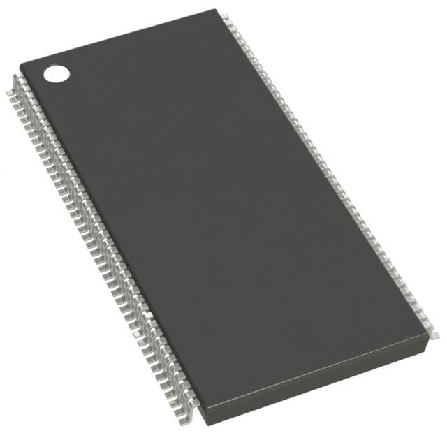
IS42S32800D-75ETL-TR
| Part Description |
IC DRAM 256MBIT PAR 86TSOP II |
|---|---|
| Quantity | 1,067 Available (as of June 15, 2026) |

| Product Category | Memory |
|---|---|
| Manufacturer | Integrated Silicon Solution Inc |
| Manufacturing Status | Obsolete |
| Manufacturer Standard Lead Time | Contact Us |
| Datasheet |
Specifications & Environmental
| Device Package | 86-TSOP II | Memory Format | DRAM | Technology | SDRAM | ||
|---|---|---|---|---|---|---|---|
| Memory Size | 256 Mbit | Access Time | 5.5 ns | Grade | Commercial | ||
| Clock Frequency | 133 MHz | Voltage | 3V ~ 3.6V | Memory Type | Volatile | ||
| Operating Temperature | 0°C ~ 70°C (TA) | Write Cycle Time Word Page | N/A | Packaging | 86-TFSOP (0.400", 10.16mm Width) | ||
| Mounting Method | Volatile | Memory Interface | Parallel | Memory Organization | 8M x 32 | ||
| Moisture Sensitivity Level | 3 (168 Hours) | RoHS Compliance | ROHS3 Compliant | REACH Compliance | REACH Unaffected | ||
| Qualification | N/A | ECCN | EAR99 | HTS Code | 8542.32.0024 |
Overview of IS42S32800D-75ETL-TR – IC DRAM 256MBIT PAR 86TSOP II
The IS42S32800D-75ETL-TR is a 256Mbit synchronous DRAM (SDRAM) organized as 8M × 32 with a quad-bank internal architecture. It implements a fully synchronous, pipeline architecture with all signals referenced to the rising edge of the clock, delivering predictable, clocked memory operation for 3.3V memory systems.
Designed for commercial-temperature applications (0°C to 70°C), this parallel-interface SDRAM provides programmable burst lengths and CAS latency options, suited for systems that require deterministic, high-speed DRAM operation in an 86‑pin TSOP‑II package.
Key Features
- Memory Core 256 Mbit capacity, organized as 8M × 32 and internally configured as 2M × 32 × 4 banks for bank interleaving and hidden precharge.
- Synchronous Pipeline Architecture Fully synchronous SDRAM with all inputs and outputs referenced to the clock rising edge; supports pipeline data transfer and randomized column addresses during burst access.
- Performance Clock frequency up to 133 MHz with access time as low as 5.5 ns (CL = 2 for the -75 device); programmable CAS latency (2, 3 clocks).
- Burst and Access Control Programmable burst lengths (1, 2, 4, 8, full page) and selectable burst sequence (sequential/interleave), with burst termination via burst stop or auto precharge.
- Refresh and Power Modes Auto Refresh (CBR) and Self Refresh support; refresh counts per datasheet options (4K cycles) with specified refresh intervals.
- Interface and Logic Levels LVTTL-compatible I/O for control and data signals; parallel memory interface for conventional SDRAM bus integration.
- Power Single power supply operation at 3.3 V (specified 3.0 V to 3.6 V).
- Package and Temperature 86‑pin TSOP‑II (10.16 mm width) package; commercial operating temperature range 0°C to 70°C (TA).
Typical Applications
- System Memory Subsystems Use as main or auxiliary DRAM in 3.3V synchronous memory systems requiring 256Mbit density and predictable clocked operation.
- Buffer and Burst Storage High-speed burst reads/writes and programmable burst sequencing make it suitable for buffer memory in parallel-interface data paths.
- Memory Expansion Modules Integration into memory modules or board-level expansions where an 86‑pin TSOP‑II footprint and commercial temperature rating are required.
Unique Advantages
- Quad‑Bank Architecture: Enables bank interleaving and hidden row precharge to improve effective throughput during burst operations.
- Flexible Burst Control: Programmable burst lengths and sequence options provide adaptable transfer patterns for varied data throughput needs.
- Deterministic Synchronous Operation: All signals registered to the clock edge support predictable timing and easy timing analysis in synchronous systems.
- Commercial Temperature Support: Rated for 0°C to 70°C for designs targeting standard commercial environments.
- Industry‑Standard Voltage: 3.3 V single-supply operation (3.0 V–3.6 V range) aligns with common SDRAM power rails.
- Compact TSOP‑II Package: 86‑pin TSOP‑II package (10.16 mm width) for board-level integration where space and conventional SO‑type footprints are used.
Why Choose IC DRAM 256MBIT PAR 86TSOP II?
The IS42S32800D-75ETL-TR delivers a synchronous, pipeline SDRAM solution with the performance and control needed for predictable, clocked memory designs. Its 8M × 32 organization, quad-bank architecture, and programmable burst/CAS options provide design flexibility for systems that require high-rate burst transfers and predictable timing.
This device is aimed at designers building 3.3V synchronous memory systems on a commercial temperature platform who need a 256Mbit parallel SDRAM in an 86‑pin TSOP‑II package. Its combination of synchronous operation, refresh modes, and LVTTL interface supports integration into established memory subsystems with standard power and timing requirements.
Request a quote or submit a product inquiry to obtain pricing, lead time, and availability for IS42S32800D-75ETL-TR.