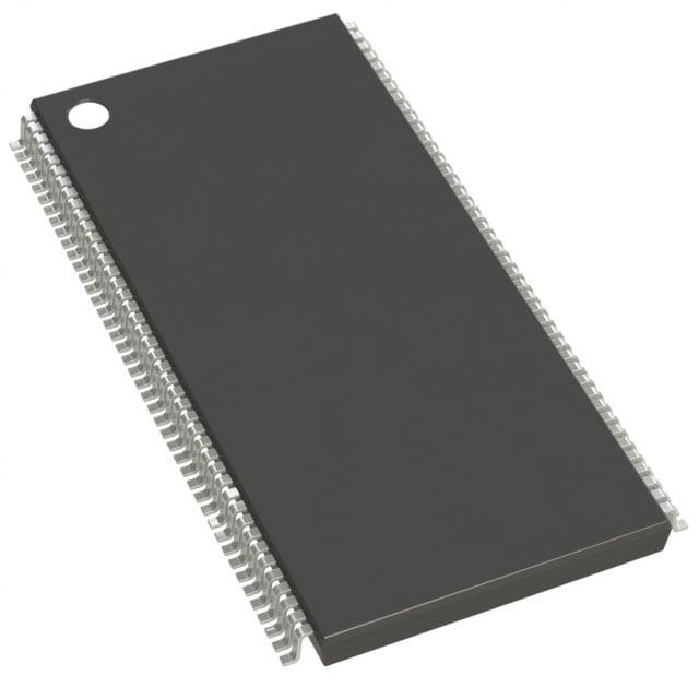
IS42S32800D-75ETLI-TR
| Part Description |
IC DRAM 256MBIT PAR 86TSOP II |
|---|---|
| Quantity | 632 Available (as of June 18, 2026) |

| Product Category | DRAM Memory |
|---|---|
| Manufacturer | Integrated Silicon Solution Inc |
| Manufacturing Status | Obsolete |
| Manufacturer Standard Lead Time | Contact Us |
| Datasheet |
Specifications & Environmental
| Device Package | 86-TSOP II | Memory Format | DRAM | Technology | SDRAM | ||
|---|---|---|---|---|---|---|---|
| Memory Size | 256 Mbit | Access Time | 5.5 ns | Grade | Industrial | ||
| Clock Frequency | 133 MHz | Voltage | 3V ~ 3.6V | Memory Type | Volatile | ||
| Operating Temperature | -40°C ~ 85°C (TA) | Write Cycle Time Word Page | N/A | Packaging | 86-TFSOP (0.400", 10.16mm Width) | ||
| Mounting Method | Volatile | Memory Interface | Parallel | Memory Organization | 8M x 32 | ||
| Moisture Sensitivity Level | 3 (168 Hours) | RoHS Compliance | ROHS3 Compliant | REACH Compliance | REACH Unaffected | ||
| Qualification | N/A | ECCN | EAR99 | HTS Code | 8542.32.0024 |
Overview of IS42S32800D-75ETLI-TR – IC DRAM 256MBIT PAR 86TSOP II
The IS42S32800D-75ETLI-TR is a 256 Mbit synchronous DRAM (SDRAM) device organized as 8M × 32 (2M × 32 × 4 banks). It implements a fully synchronous, pipeline architecture with all signals referenced to the rising edge of the clock for predictable high-speed operation.
Designed for systems that require parallel SDRAM buffering and burst access, the device offers programmable burst lengths and sequence options, LVTTL I/O compatibility, and a compact 86‑pin TSOP‑II package with a 10.16 mm width.
Key Features
- Core / Memory Architecture Quad‑bank synchronous DRAM organized as 2M × 32 × 4 banks (8M × 32 total, 256 Mbit) to support interleaved bank operation and pipelined access.
- Performance Supports a clock frequency up to 133 MHz for the -75E option with CAS‑latency 2 and an access time of 5.5 ns (CAS‑latency = 2).
- Programmable Burst and CAS Options Programmable burst length (1, 2, 4, 8, full page) and burst sequence (sequential or interleave). CAS latency selectable between 2 and 3 clocks.
- Refresh and Power Modes Auto‑refresh and self‑refresh supported; refresh cycles specified as 4096 counts with timing options of 16 ms (A2 grade) or 64 ms (Commercial/Industrial/A1 grade) per datasheet options.
- Interface and Signaling LVTTL‑compatible inputs/outputs and parallel memory interface with random column address capability every clock cycle for flexible burst access.
- Power Single 3.3 V supply nominal (specified supply range 3.0 V to 3.6 V / 3.3 V ±0.3 V in datasheet).
- Package and Mounting 86‑pin TSOP‑II (86‑TFSOP) package, 0.400" (10.16 mm) width, suitable for surface‑mount applications.
- Operating Temperature Specified operating ambient range: −40 °C to +85 °C (TA).
Typical Applications
- High‑speed buffering Use in systems requiring synchronous burst transfers and low access latency for temporary data storage and buffering.
- Memory subsystems Integration into parallel SDRAM memory banks where programmable burst length and interleaved bank access improve throughput.
- Embedded processing platforms Suitable for embedded designs that require a compact 86‑pin TSOP‑II packaged SDRAM with LVTTL interface and standard 3.3 V operation.
Unique Advantages
- Flexible burst control: Programmable burst lengths and sequence modes enable tailored transfer patterns to match system data flow.
- Low access latency: 5.5 ns access time at the -75E option (CAS‑latency = 2) supports responsive read operations in time‑sensitive designs.
- Interleaved bank architecture: Quad‑bank internal organization allows hidden row access/precharge and improved effective throughput during burst operations.
- Standard voltage and signaling: 3.3 V single‑supply operation with LVTTL I/O simplifies integration into common memory subsystems.
- Compact footprint: 86‑TSOP II package provides high density in a small surface‑mount form factor for space‑constrained PCBs.
Why Choose IS42S32800D-75ETLI-TR?
The IS42S32800D-75ETLI-TR delivers a compact, fully synchronous 256 Mbit SDRAM solution with programmable burst and CAS settings, LVTTL I/O, and a quad‑bank architecture that helps maintain high sustained data throughput. Its 3.3 V single‑supply operation and standard TSOP‑II footprint make it suitable for integration into a wide range of parallel memory subsystems.
This device is well suited to designers and procurement teams seeking a verifiable, specification‑driven DRAM component for embedded platforms and high‑speed buffering applications where predictable timing, selectable latency, and compact packaging are required.
Request a quote or submit a quote request to obtain pricing, lead time, and availability for the IS42S32800D-75ETLI-TR.