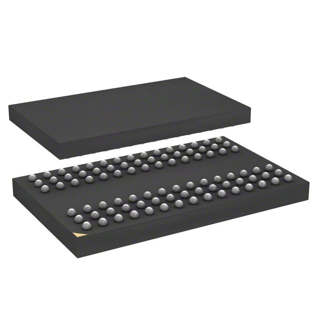
IS42S32800D-7BLI
| Part Description |
IC DRAM 256MBIT PAR 90TFBGA |
|---|---|
| Quantity | 521 Available (as of June 15, 2026) |

| Product Category | DRAM Memory |
|---|---|
| Manufacturer | Integrated Silicon Solution Inc |
| Manufacturing Status | Obsolete |
| Manufacturer Standard Lead Time | Contact Us |
| Datasheet |
Specifications & Environmental
| Device Package | 90-TFBGA (8x13) | Memory Format | DRAM | Technology | SDRAM | ||
|---|---|---|---|---|---|---|---|
| Memory Size | 256 Mbit | Access Time | 5.4 ns | Grade | Industrial | ||
| Clock Frequency | 143 MHz | Voltage | 3V ~ 3.6V | Memory Type | Volatile | ||
| Operating Temperature | -40°C ~ 85°C (TA) | Write Cycle Time Word Page | N/A | Packaging | 90-TFBGA | ||
| Mounting Method | Volatile | Memory Interface | Parallel | Memory Organization | 8M x 32 | ||
| Moisture Sensitivity Level | 3 (168 Hours) | RoHS Compliance | ROHS3 Compliant | REACH Compliance | REACH Unaffected | ||
| Qualification | N/A | ECCN | EAR99 | HTS Code | 8542.32.0024 |
Overview of IS42S32800D-7BLI – IC DRAM 256MBIT PAR 90TFBGA
The IS42S32800D-7BLI is a 256Mbit synchronous DRAM device organized as 8M × 32 with an internal quad-bank architecture (2M × 32 × 4 banks). It implements a pipelined, fully synchronous interface with all signals referenced to the rising edge of the clock for predictable timing in parallel memory systems.
Designed for systems that require high-speed burst transfers and low-latency access, the device offers programmable burst lengths and sequences, selectable CAS latency, and support for auto- and self-refresh modes—making it suitable for embedded and industrial designs that use parallel SDRAM memory.
Key Features
- Memory Core 256 Mbit SDRAM organized as 8M × 32 with internal configuration of 2M × 32 × 4 banks for bank interleaving and improved access concurrency.
- Performance Supports a clock frequency of 143 MHz and an access time from clock of 5.4 ns (CAS latency = 3), enabling high-speed burst transfers.
- Programmable Burst and Latency Programmable burst lengths (1, 2, 4, 8, full page) and burst sequence (sequential/interleave) with selectable CAS latency of 2 or 3 clocks for flexible throughput/latency tradeoffs.
- Refresh and Power Modes Auto Refresh and Self Refresh supported; refresh options include 4096 cycles per 16 ms (A2) or per 64 ms (Commercial/Industrial/A1) as specified in the device options.
- Interface and Logic Fully synchronous operation with LVTTL-compatible I/O and a parallel memory interface referenced to CLK for deterministic timing.
- Supply and Operating Range Single power supply operation at 3.3 V ±0.3 V (listed supply range 3.0 V – 3.6 V) and specified operating temperature range of −40 °C to +85 °C (TA).
- Package 90-ball TF‑BGA package (8 × 13) for compact board-level integration.
- Bank Management Internal bank architecture and autoprecharge capability to hide row access/precharge and support random column addressing every clock cycle during burst access.
Typical Applications
- Embedded systems Parallel SDRAM memory for applications requiring predictable synchronous access and configurable burst behavior.
- Industrial control Memory for industrial devices benefitting from a −40 °C to +85 °C operating range and synchronous burst performance.
- High-speed buffering Frame buffers or data stream buffers that leverage programmable burst lengths and bank interleaving for sustained throughput.
Unique Advantages
- Flexible burst control: Programmable burst lengths and selectable sequential or interleave sequences let designers tune transfer behavior to application needs.
- Low-latency synchronous access: CAS latency options (2 or 3) and a 143 MHz clock option with 5.4 ns access time (CL=3) provide predictable, low-latency reads.
- Robust refresh options: Auto and self-refresh support with documented refresh cycles (4K per 16 ms or 64 ms depending on grade) simplify system power management.
- Industrial temperature support: Specified −40 °C to +85 °C operating range aligns with many industrial deployment requirements.
- Compact BGA footprint: 90-TFBGA (8×13) package enables high-density board designs while providing a parallel memory interface.
Why Choose IS42S32800D-7BLI?
The IS42S32800D-7BLI delivers a documented synchronous DRAM solution that combines a 256 Mbit density, quad-bank organization, and configurable burst and latency settings to meet a range of performance and timing requirements. Its 3.3 V supply compatibility, LVTTL interface, and −40 °C to +85 °C operating range make it a practical choice for embedded and industrial designs needing parallel SDRAM memory.
With clear timing parameters and refresh options provided in the device specification, this SDRAM is suited for designs that require deterministic synchronous behavior, selectable throughput/latency tradeoffs, and compact board-level integration in a 90-TFBGA package.
Request a quote or contact sales to discuss availability and pricing for IS42S32800D-7BLI and to obtain full technical documentation or volume pricing information.