IS42S32800D-7BI
| Part Description |
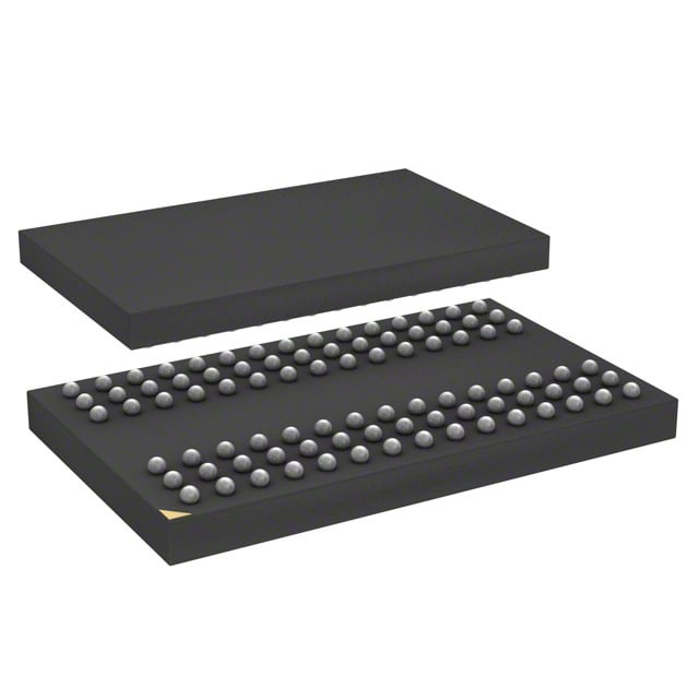
IC DRAM 256MBIT PAR 90TFBGA |
|---|---|
| Quantity | 574 Available (as of June 15, 2026) |

| Product Category | Memory |
|---|---|
| Manufacturer | Integrated Silicon Solution Inc |
| Manufacturing Status | Obsolete |
| Manufacturer Standard Lead Time | Contact Us |
| Datasheet |
Specifications & Environmental
| Device Package | 90-TFBGA (8x13) | Memory Format | DRAM | Technology | SDRAM | ||
|---|---|---|---|---|---|---|---|
| Memory Size | 256 Mbit | Access Time | 5.4 ns | Grade | Industrial | ||
| Clock Frequency | 143 MHz | Voltage | 3V ~ 3.6V | Memory Type | Volatile | ||
| Operating Temperature | -40°C ~ 85°C (TA) | Write Cycle Time Word Page | N/A | Packaging | 90-TFBGA | ||
| Mounting Method | Volatile | Memory Interface | Parallel | Memory Organization | 8M x 32 | ||
| Moisture Sensitivity Level | 3 (168 Hours) | RoHS Compliance | ROHS3 Compliant | REACH Compliance | REACH Unaffected | ||
| Qualification | N/A | ECCN | EAR99 | HTS Code | 8542.32.0024 |
Overview of IS42S32800D-7BI – IC DRAM 256MBIT PAR 90TFBGA
The IS42S32800D-7BI is a 256Mbit synchronous DRAM (SDRAM) organized as 8M × 32 with a quad-bank architecture and pipeline design for high-speed, synchronous data transfer. It implements a parallel memory interface with LVTTL-compatible I/O and is optimized for systems that require a compact 90‑TFBGA package and a 3.3V-class power supply.
This device targets designs requiring programmable burst operation, selectable CAS latency, and robust refresh/power modes, providing a balance of performance and predictable timing for commercial and industrial temperature applications.
Key Features
- Core / Architecture 256Mbit SDRAM organized as 2M × 32 × 4 banks (8M × 32) with internal bank interleaving and pipeline architecture to support high-speed synchronous operation.
- Performance Clock frequency up to 143 MHz (device -7 speed grade) with an access time from clock of 5.4 ns at CAS latency = 3.
- Programmable Burst and Latency Programmable burst lengths (1, 2, 4, 8, full page), sequential/interleave burst sequences, and programmable CAS latency options (2 or 3 clocks) for flexible data transfer patterns.
- Refresh and Power Management Auto Refresh and Self Refresh support; refresh intervals documented for commercial/industrial and A‑grade options (4K refresh cycles per specified interval).
- Interface and Signaling Parallel memory interface with LVTTL-compatible I/O and support for random column address every clock cycle.
- Power Single power supply operation around 3.3 V (specified 3.0 V to 3.6 V range; datasheet specifies 3.3 V ± 0.3 V).
- Package and Temperature Supplied in a 90‑TFBGA (90‑ball, 8×13) package; specified operating temperature range -40 °C to +85 °C (TA) for the listed device variant.
Typical Applications
- Embedded systems Acts as synchronous system memory where predictable timing, burst transfers, and selectable CAS latency are required.
- Networking and communications equipment Supports high-speed burst read/write patterns and random column access for packet buffering and streaming data tasks.
- Industrial control Operates over -40 °C to +85 °C, suitable for industrial-grade designs that require SDRAM with self‑refresh and auto‑refresh capabilities.
- Consumer electronics Provides a compact 90‑TFBGA footprint and configurable burst modes for compact board designs with synchronous memory needs.
Unique Advantages
- High-speed synchronous operation: 143 MHz clock frequency (‑7 speed grade) and pipeline architecture deliver tight timing and predictable access performance.
- Flexible data transfer modes: Programmable burst lengths and sequence plus programmable CAS latency allow tuning for different throughput and latency requirements.
- Robust refresh and power modes: Auto Refresh and Self Refresh reduce system overhead for refresh management and support power saving.
- Standard 90‑TFBGA packaging: Compact 90-ball (8×13) TF‑BGA package enables high-density board integration while maintaining ball-grid reliability.
- 3.3V-class compatibility: Operates within a 3.0 V to 3.6 V supply window (datasheet specifies 3.3 V ±0.3 V), matching common system power rails.
- Industrial temperature capability: Device variant specified for -40 °C to +85 °C operation, supporting temperature‑sensitive deployments.
Why Choose IS42S32800D-7BI?
The IS42S32800D-7BI provides a compact, configurable 256Mbit SDRAM solution from Integrated Silicon Solution, Inc., combining a synchronous pipeline architecture with programmable burst and latency options. Its LVTTL-compatible parallel interface, 3.3V-class supply compatibility, and documented timing (5.4 ns access at CL=3) make it a practical choice for designs that need deterministic SDRAM behavior in a space-efficient 90‑TFBGA package.
This device is well suited to engineers designing commercial or industrial systems that require scalable memory bandwidth, selectable latency/burst behavior, and reliable refresh/power modes. Its documented operating range and package option help simplify BOM decisions for long‑lifecycle hardware projects.
Request a quote or submit an inquiry for pricing and availability of IS42S32800D-7BI to discuss lead times and volume options.